ALLPCB


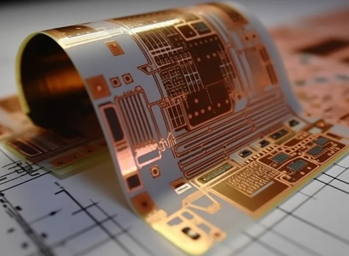
In the fast-evolving world of electronics, flexible printed circuit boards (PCBs) are key to creating smaller, lighter, and more versatile devices. One critical process in flex PCB manufacturing is laser drilling, a technology that ensures high density and reliability in via drilling for flex circuits. If you're looking to understand how laser drilling works for flexible materials or why it's a game-changer for achieving precision, you're in the right place. This blog dives deep into the benefits, processes, and applications of laser drilling in flex PCB production, focusing on long-tail keywords like laser drilling flexible PCB, flex PCB manufacturing, via drilling flex circuits, and laser ablation flexible materials.
What Is Laser Drilling in Flex PCB Manufacturing?
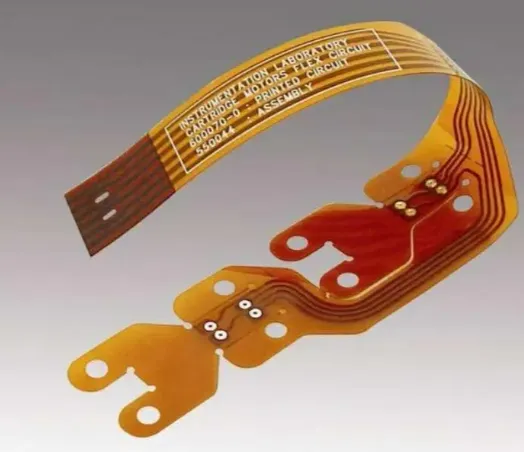
Laser drilling is a cutting-edge technique used to create microvias and holes in flexible PCBs with pinpoint accuracy. Unlike traditional mechanical drilling, which can struggle with the delicate and thin nature of flexible materials, laser drilling uses a focused beam of light to ablate or vaporize material. This method is ideal for via drilling in flex circuits because it minimizes damage to surrounding areas and allows for incredibly small hole sizes, often down to 25 micrometers or less.
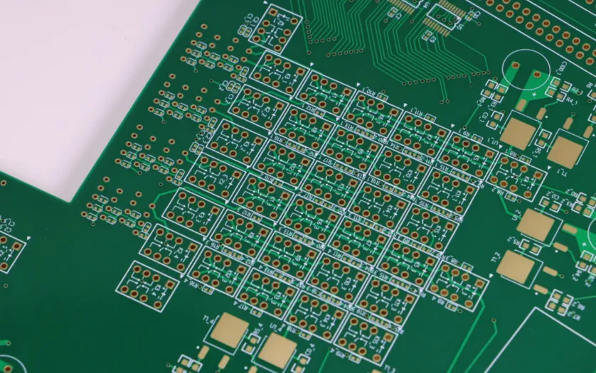
In flex PCB manufacturing, achieving high density means packing more components into a smaller space. Laser drilling enables this by creating precise microvias that connect multiple layers in a compact design. Whether it's for wearable devices, medical equipment, or automotive systems, the reliability of these connections is vital, and laser ablation of flexible materials ensures consistent performance even under stress.
Why Choose Laser Drilling for Flexible PCBs?
Laser drilling offers several advantages over traditional methods when it comes to flex PCB manufacturing. Let's explore why this technology is becoming the go-to choice for engineers aiming for high density and reliability.
1. Precision for High-Density Designs
Flexible PCBs often need to fit into tight spaces, requiring intricate designs with tiny vias. Laser drilling can achieve hole diameters as small as 20-30 micrometers, far smaller than what mechanical drilling can manage (typically limited to 100 micrometers or more). This precision supports high-density interconnects, allowing more circuits to be packed into a smaller footprint. For example, in a wearable fitness tracker, laser-drilled microvias can connect multiple layers without increasing the device's size.
2. Minimal Damage to Flexible Materials
Flexible materials like polyimide or polyester are prone to tearing or deformation during mechanical drilling. Laser ablation of flexible materials avoids physical contact, reducing the risk of cracks or delamination. The heat-affected zone (HAZ) in laser drilling is also minimal, often less than 10 micrometers, ensuring the integrity of the surrounding material remains intact.
3. Enhanced Reliability for Flex Circuits
Reliability is non-negotiable in applications like medical implants or aerospace systems. Laser drilling for flexible PCBs creates clean, uniform holes without burrs or debris, which can cause short circuits or signal interference. Studies have shown that laser-drilled vias in flex circuits can maintain signal integrity at speeds up to 10 Gbps, making them suitable for high-performance electronics.
How Does Laser Drilling Work in Flex PCB Manufacturing?
The process of laser drilling in flex PCB manufacturing involves using a concentrated laser beam to remove material layer by layer. Here's a step-by-step breakdown of how it works for via drilling in flex circuits:
- Setup and Programming: The design file for the flexible PCB is loaded into the laser drilling system. This file specifies the exact locations and sizes of the vias needed.
- Laser Beam Focus: A high-energy laser, often a UV or CO2 type, is focused on the target area. UV lasers are preferred for their precision, with wavelengths around 355 nm, ideal for ablating thin flexible materials.
- Material Ablation: The laser beam vaporizes the material at the focal point, creating a hole. The process is controlled to ensure the depth matches the design, often stopping at a specific layer in multilayer flex PCBs.
- Cleaning and Inspection: After drilling, any residue is cleaned, and the board undergoes inspection to verify hole dimensions and placement accuracy, often achieving tolerances of ±5 micrometers.
Laser ablation of flexible materials is particularly effective because it can handle varying thicknesses, from 25 micrometers to over 100 micrometers, without compromising quality. This adaptability makes it a cornerstone of modern flex PCB manufacturing.
Applications of Laser Drilling in Flexible PCBs
Laser drilling for flexible PCBs is transforming industries that demand compact, reliable, and high-performance electronics. Here are some key applications where this technology shines:
1. Wearable Technology
Wearables like smartwatches and fitness bands rely on flexible PCBs to conform to curved shapes. Laser-drilled microvias enable dense layouts, supporting features like heart rate sensors and wireless communication in a tiny form factor. The reliability of these vias ensures consistent performance even with constant bending.
2. Medical Devices
In medical applications, such as pacemakers or diagnostic tools, space is limited, and reliability is critical. Laser drilling allows for high-density interconnects in flex circuits, ensuring stable signal transmission (e.g., impedance control within 50 ohms ±10%) while withstanding the body's dynamic environment.
3. Automotive Electronics
Modern vehicles use flexible PCBs in sensors, displays, and control systems. Laser drilling supports the creation of robust vias that endure vibration and temperature swings, maintaining signal speeds up to 5 Gbps for advanced driver-assistance systems (ADAS).
Challenges in Laser Drilling for Flex PCBs
While laser drilling offers unmatched precision, it’s not without challenges. Understanding these hurdles can help engineers optimize their designs for flex PCB manufacturing.
1. Cost Considerations
Laser drilling equipment requires significant investment, and the process can be slower than mechanical drilling for larger holes. However, the cost is often justified by the superior quality and reduced failure rates in high-density designs.
2. Material Sensitivity
Some flexible materials may absorb laser energy differently, leading to inconsistent results if not properly calibrated. For instance, polyimide films require specific laser parameters (e.g., pulse duration below 10 nanoseconds) to avoid charring.
3. Depth Control
In multilayer flex PCBs, controlling the laser to stop at the correct depth is crucial. Advanced systems use real-time feedback to achieve depth accuracy within 2-3 micrometers, but this requires skilled operators and precise setup.
Best Practices for Via Drilling in Flex Circuits
To maximize the benefits of laser drilling in flex PCB manufacturing, engineers should follow these best practices:
- Optimize Design Files: Ensure via locations and sizes are clearly defined in the design software to avoid errors during drilling. Target microvia diameters between 25-50 micrometers for optimal results.
- Choose the Right Material: Select flexible substrates compatible with laser ablation, such as polyimide, which handles thermal stress well during drilling.
- Work with Experienced Partners: Collaborate with manufacturers who have advanced laser drilling capabilities and can provide consistent quality across production runs.
- Test for Reliability: After drilling, conduct thorough testing for signal integrity and impedance, ensuring values meet specifications (e.g., impedance within ±5% of target).
Future Trends in Laser Drilling for Flexible PCBs
The field of laser drilling is advancing rapidly, driven by the demand for smaller, more efficient electronics. Here are some trends shaping the future of via drilling in flex circuits:
1. Ultrafast Laser Systems
New ultrafast lasers with pulse durations in the femtosecond range (10^-15 seconds) are emerging. These systems further reduce the heat-affected zone, enabling even finer holes (below 10 micrometers) in flexible materials without thermal damage.
2. Automation and AI Integration
Automation in laser drilling systems, combined with AI for real-time adjustments, is improving throughput and accuracy. This means faster production times for flex PCB manufacturing while maintaining tolerances as tight as ±2 micrometers.
3. Green Laser Technology
Green lasers, operating at wavelengths around 532 nm, are gaining traction for their ability to drill through a wider range of flexible materials with minimal residue. This technology promises cleaner vias and reduced post-processing steps.
Conclusion: Elevating Flex PCB Manufacturing with Laser Drilling
Laser drilling for flexible PCBs is revolutionizing the way we design and produce high-density, reliable electronics. By enabling precise via drilling in flex circuits and effective laser ablation of flexible materials, this technology meets the demands of modern applications—from wearables to automotive systems. While challenges like cost and material sensitivity exist, the benefits of precision, minimal damage, and enhanced reliability make laser drilling an essential tool in flex PCB manufacturing.
At ALLPCB, we're committed to leveraging advanced technologies like laser drilling to deliver top-quality flexible PCBs for your projects. Whether you're working on a compact wearable or a critical medical device, our expertise ensures your designs achieve the density and performance you need. Explore our services to see how we can support your next innovation with cutting-edge flex PCB solutions.