 ALLPCB


Definition and Industry Standards
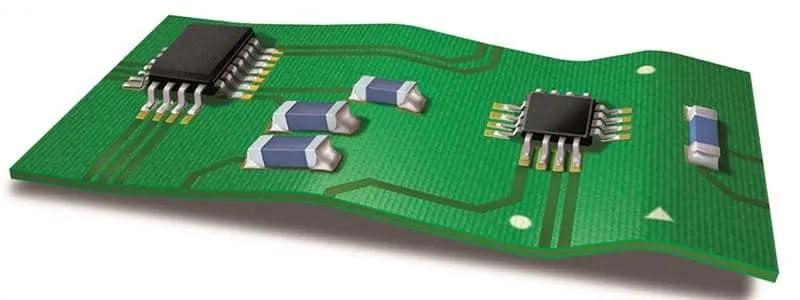
Printed Circuit Board (PCB) warpage refers to the phenomenon that the plane of the PCB is bent or deformed due to various reasons during the manufacturing, storage or use of the PCB. This deformation may be local or overall, and is usually manifested as the PCB no longer remaining flat.
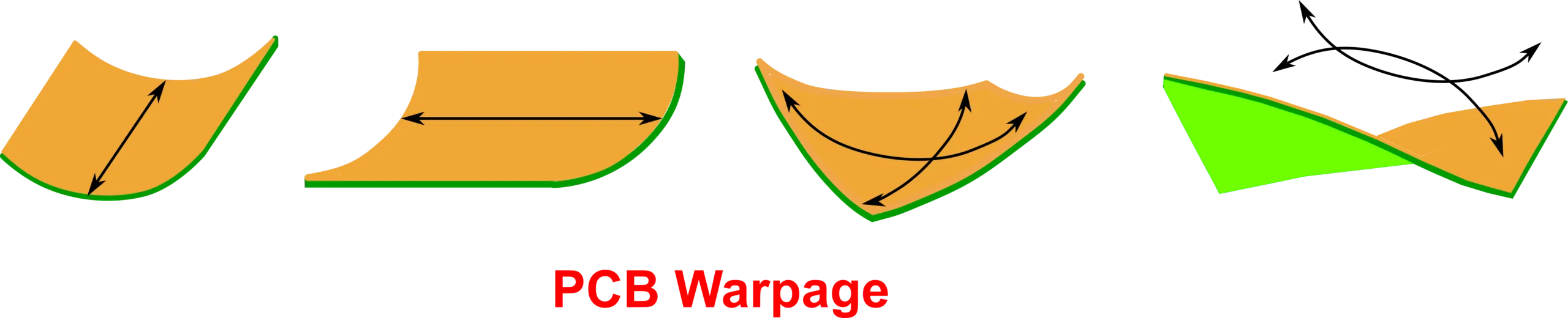
Different application fields and industries have different requirements for PCB warpage. Generally speaking, for ordinary PCBs, it is usually required that the warpage within a certain size range should not exceed 0.75% to 1%. For example, for a PCB with a size of 300mm×300mm, its warpage should generally not exceed 2.25mm to 3mm. For some electronic products with high precision requirements, such as high-end servers, communication equipment, etc., the PCB warpage requirements may be more stringent, usually required to be below 0.5%. In the automotive electronics industry, since cars are affected by vibration, temperature changes and other factors during driving, the reliability requirements for PCBs are relatively high. Generally speaking, the warpage of PCBs for automotive electronics is required to be less than 0.7%. In the aerospace field, the quality and reliability requirements for PCBs are extremely high, and the warpage requirements are usually less than 0.3%.
Suggested Reading: What Causes PCB Warpage?
Adverse effects of PCB warping
1. Impact on the installation of electronic components
During the electronic assembly process, a warped PCB makes it difficult to install components. Automatic placement machines may not be able to accurately place components in the intended position, resulting in reduced installation accuracy. When installing manually, it also takes more time and effort to adjust the position of components, thereby reducing production efficiency.
Components installed on warped PCBs may be subject to uneven stress, which may affect the welding quality of components and increase the risk of welding defects such as cold soldering and desoldering.
2. Impact on electrical performance
PCB warping may cause changes in the length and spacing of lines on the PCB, thereby changing the impedance characteristics of the circuit. This may cause delay, attenuation and distortion of signal transmission, reducing the quality and integrity of the signal.
In high-frequency circuits, this effect is particularly significant, which may cause signal reflection and interference, affecting the normal operation of the circuit.
3. Impact on equipment accuracy and performance
For some electronic products with high precision requirements, such as medical equipment, aerospace equipment, etc., PCB warping may affect the overall accuracy and performance of the equipment.
For example, in medical equipment, PCB warping may cause the measurement error of the sensor to increase, affecting the accuracy of the diagnostic results. In aerospace equipment, PCB warping may affect the performance of key equipment such as navigation systems and communication systems, endangering flight safety.
4. Impact on reliability and life
Since warping will cause uneven stress on components on the PCB, long-term use may cause fatigue damage and failure of components.
At the same time, warping may also cause poor fit between the PCB and the casing, resulting in reduced sealing of electronic products, which are easily affected by external environmental factors such as dust and moisture, thereby reducing the reliability and life of electronic products.
Recommended Reading: Large PCB Panel (≥500mm) Warpage Control
Conclusion
In short, PCB warping is an issue that needs to be highly valued, which may have many adverse effects on the production and use of electronic products. Understanding the causes, effects and coping strategies of PCB warping is crucial to improving the quality and reliability of electronic products. As a professional PCB manufacturer, ALLPCB strictly controls and inspects PCB warping during the manufacturing process of PCBs, and has zero tolerance for PCB warping. At the same time, ALLPCB's after-sales team will also actively negotiate with users to deal with problems and do their best to reduce losses for users.


