 ALLPCB


In the fast-paced world of electronics design, speed and adaptability are everything. If you're an engineer or designer looking to bring innovative products to market quickly, you’ve likely heard of rigid-flex PCBs and quick-turn prototyping. But what makes these technologies so powerful together? Rigid-flex PCBs combine the durability of rigid boards with the adaptability of flexible circuits, while quick-turn services slash prototyping timelines. This powerful duo is revolutionizing rapid prototyping by allowing complex designs to be tested and iterated at lightning speed.
In this blog, we’ll dive deep into the world of rigid-flex PCBs, explore their benefits for dynamic and static applications, and explain how quick-turn services can accelerate your project. Whether you're working on wearables, medical devices, or IoT gadgets, understanding how to leverage rigid-flex PCBs and rapid prototyping can give you a competitive edge. Let’s explore how these technologies are bending the rules of design and manufacturing.
What Are Rigid-Flex PCBs?
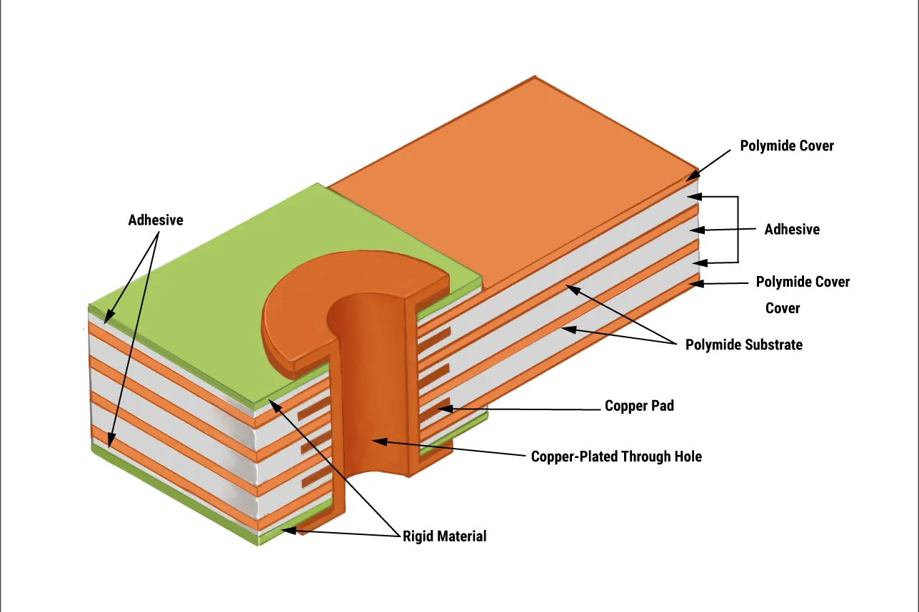
Rigid-flex PCBs are hybrid circuit boards that integrate rigid and flexible sections into a single design. The rigid parts provide structural support and house components, while the flexible sections allow the board to bend or fold, fitting into tight or irregular spaces. This unique combination eliminates the need for connectors or cables between rigid and flexible areas, reducing weight, space, and potential failure points.
These boards are ideal for applications where space is limited or where the PCB must endure repeated bending. They come in two main types based on their bending behavior: dynamic flex PCBs, which are designed for frequent bending (like in foldable devices), and static flex PCBs, which are bent into a fixed shape during installation and remain static (like in compact medical tools). By understanding the differences between dynamic and static flex PCBs, designers can choose the right solution for their specific needs.
Key Benefits of Rigid-Flex PCBs in Modern Design
Rigid-flex PCBs offer a range of advantages that make them a top choice for cutting-edge electronics. Here are some of the standout benefits:
- Space Efficiency: By combining rigid and flexible areas, these boards can fold into compact shapes, saving up to 60% of space compared to traditional rigid PCB designs. This is critical for small devices like wearables or IoT sensors.
- Durability: The integrated design reduces the number of connectors, lowering the risk of connection failures. Studies show that rigid-flex designs can improve reliability by up to 30% in high-vibration environments like automotive applications.
- Cost-Effectiveness in Assembly: Fewer components and simpler assembly processes can cut manufacturing costs by 20-30%, especially for complex designs that would otherwise require multiple boards and connectors.
- Versatility in Bending: Whether you need a dynamic flex PCB for constant motion or a static flex PCB for a one-time bend, rigid-flex designs adapt to a wide range of mechanical requirements.
These benefits make rigid-flex PCBs a go-to solution for industries like aerospace, medical, and consumer electronics, where reliability and compact design are non-negotiable.
Dynamic Flex PCBs vs. Static Flex PCBs: What’s the Difference?
When designing with rigid-flex PCBs, one of the first decisions is whether to use a dynamic or static flex configuration. Let’s break down the differences to help you choose the right type for your project.
Dynamic Flex PCBs
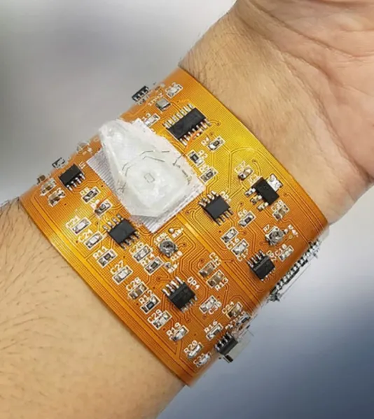
Dynamic flex PCBs are built to handle repeated bending or flexing over thousands of cycles without failure. They’re often used in applications like foldable smartphones, robotic arms, or wearable fitness trackers. The flexible materials in these designs, such as polyimide, are chosen for their ability to withstand stress, with typical bend radii as tight as 0.5mm for single-layer flex circuits.
Key considerations for dynamic flex PCBs include:
- Ensuring copper traces are placed in neutral bending zones to minimize strain.
- Using thinner materials to reduce stress during flexing, often with thicknesses under 0.1mm for the flexible layers.
- Testing for a minimum of 10,000 bend cycles to ensure longevity in high-use applications.
Static Flex PCBs
Static flex PCBs, on the other hand, are designed to be bent into a specific shape during assembly and remain in that position for the product’s lifecycle. They’re common in devices like cameras or medical implants, where the board needs to fit into a unique form factor but won’t move once installed. These designs prioritize cost-efficiency and ease of manufacturing over repeated flexibility.
Key considerations for static flex PCBs include:
- Selecting materials with enough flexibility for a one-time bend, often with a minimum bend radius of 10 times the board thickness (e.g., 1.5mm for a 0.15mm thick flex layer).
- Reinforcing rigid areas to support components without compromising the flex zone.
- Focusing on thermal management since static designs may trap heat in confined spaces.
PCB Bending: Challenges and Best Practices
One of the defining features of rigid-flex and flexible PCBs is their ability to bend. However, PCB bending comes with challenges that must be addressed during design to avoid failures like cracked traces or delamination. Here are some critical factors to consider:
- Bend Radius: The bend radius determines how tightly a PCB can flex without damage. For dynamic flex PCBs, a smaller radius (e.g., 0.5mm) is often necessary, while static flex PCBs can handle larger radii (e.g., 1.5-2mm). Exceeding the recommended radius can cause copper traces to crack, leading to signal loss.
- Trace Layout: Copper traces should be routed perpendicular to the bend line to reduce stress. For dynamic applications, staggered or curved traces can distribute strain more evenly, reducing failure rates by up to 25%.
- Material Selection: Flexible layers often use polyimide films with dielectric constants around 3.4, ensuring signal integrity at high frequencies (up to 5 GHz in some designs). Rigid sections may use FR-4 with thicknesses of 1.6mm for stability.
By carefully designing for PCB bending, engineers can create reliable products that perform under mechanical stress while maintaining electrical performance.
Quick-Turn Prototyping: Speeding Up Innovation
In today’s competitive market, getting a product from concept to production in the shortest time possible is crucial. This is where quick-turn prototyping shines. Quick-turn services focus on delivering functional prototypes in days rather than weeks, allowing designers to test and refine rigid-flex PCB designs rapidly.
Here’s how quick-turn prototyping transforms the development process:
- Reduced Lead Times: Standard PCB manufacturing can take 2-4 weeks, but quick-turn services can deliver prototypes in as little as 24-48 hours for simpler designs or 5-7 days for complex rigid-flex boards.
- Iterative Testing: Fast prototyping enables multiple design iterations in a short period. For example, an IoT device designer might test three versions of a flexible PCB layout in under two weeks, identifying the optimal configuration for signal integrity (e.g., maintaining impedance at 50 ohms).
- Cost Savings: Early detection of design flaws through rapid prototyping can save up to 40% on development costs by avoiding expensive redesigns later in the process.
When paired with rigid-flex PCBs, quick-turn services allow engineers to experiment with innovative designs without sacrificing time-to-market goals.
How Rigid-Flex PCBs and Quick-Turn Services Work Together
The synergy between rigid-flex PCBs and quick-turn prototyping is a game-changer for rapid product development. Rigid-flex designs often involve complex layer stacks (e.g., 4-8 layers combining rigid and flexible materials) and tight tolerances, making prototyping essential to validate performance. Quick-turn services ensure that these prototypes are produced and delivered fast, even for intricate designs.
For instance, consider a wearable health monitor that requires a dynamic flex PCB to wrap around the wrist. The design might include a 4-layer stack with a flexible core of 0.05mm polyimide and rigid sections of 1.6mm FR-4 for mounting sensors. With quick-turn prototyping, the designer can receive a functional prototype in under a week, test bending durability (e.g., 20,000 cycles), and adjust trace widths to optimize signal speed (e.g., achieving 1 ns delay for critical signals).
This combination empowers engineers to push the boundaries of design while meeting tight deadlines, ensuring that innovative products reach the market faster than ever.
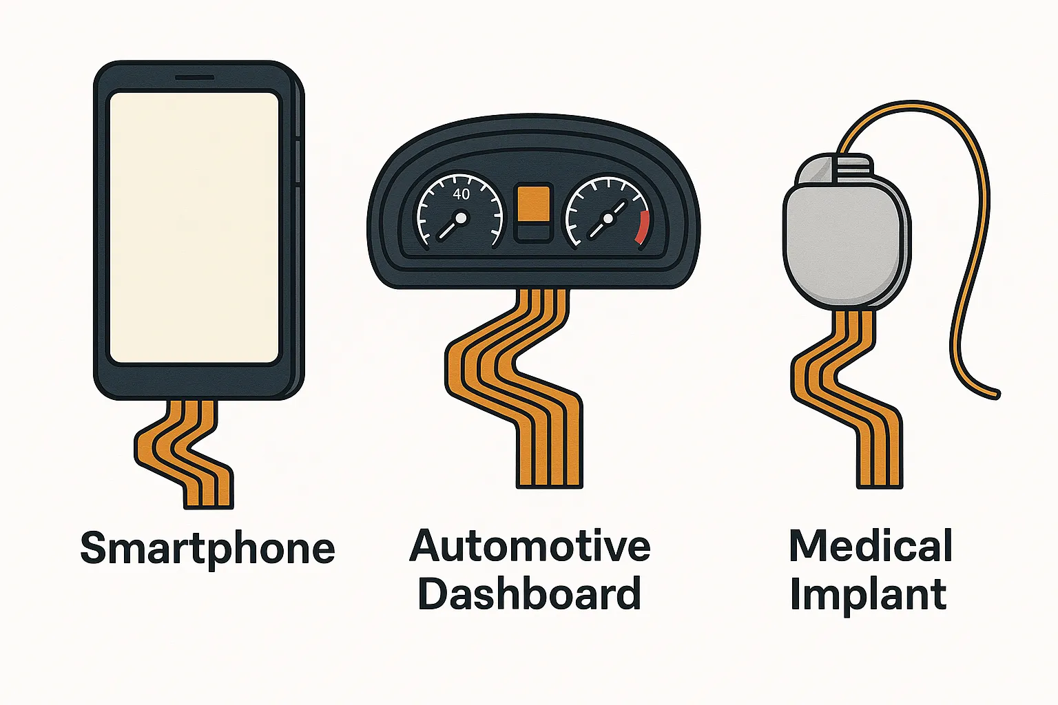
Applications of Rigid-Flex PCBs in Rapid Prototyping
Rigid-flex PCBs are transforming industries through their adaptability and reliability. Here are some key applications where they excel, especially when paired with quick-turn prototyping:
- Wearables: Devices like smartwatches use dynamic flex PCBs to conform to curved shapes, with prototypes often needed in days to meet launch schedules.
- Medical Devices: Compact tools like endoscopes rely on static flex PCBs to fit intricate designs, with rapid prototyping ensuring biocompatibility and performance are tested early.
- Automotive Systems: Rigid-flex PCBs in sensors and control units withstand vibration and heat, with quick-turn services enabling fast validation of designs for safety-critical applications.
- IoT Gadgets: Small, connected devices benefit from the space savings of rigid-flex designs, while rapid prototyping accelerates testing of wireless signal integrity (e.g., maintaining 2.4 GHz performance).
Tips for Designing Rigid-Flex PCBs for Quick-Turn Prototyping
To make the most of rigid-flex PCBs and quick-turn services, consider these practical design tips:
- Simplify Layer Stacks: While rigid-flex designs can have up to 12 layers, aim for 4-6 layers in prototypes to reduce manufacturing time and cost.
- Define Bend Areas Early: Clearly mark flexible zones in your design files to avoid miscommunication with manufacturers, ensuring proper material selection for PCB bending.
- Optimize Component Placement: Place heavy components on rigid sections to avoid stress on flexible areas, especially for dynamic flex PCBs.
- Account for Signal Integrity: Maintain controlled impedance (e.g., 50 ohms for high-speed signals) by adjusting trace widths and spacing, particularly in flexible zones where dielectric constants vary.
- Collaborate with Manufacturers: Share detailed design requirements upfront to ensure quick-turn timelines are met without compromising quality.
By following these guidelines, you can streamline the prototyping process and achieve reliable results with your rigid-flex PCB designs.
Conclusion: Bending the Rules for Faster Innovation
Rigid-flex PCBs and quick-turn prototyping are reshaping the landscape of electronics design. By combining the versatility of rigid-flex technology with the speed of rapid prototyping, engineers can create compact, reliable, and innovative products faster than ever before. Whether you’re working with dynamic flex PCBs for wearable tech or static flex PCBs for medical tools, this powerful pairing offers unmatched flexibility and efficiency.
Understanding the nuances of PCB bending, material selection, and design optimization is key to unlocking the full potential of these technologies. With the right approach, you can bend the rules of traditional prototyping, turning complex ideas into market-ready solutions in record time. At ALLPCB, we’re committed to supporting your journey with high-quality manufacturing and fast turnaround times, helping you stay ahead in a competitive industry.


