 ALLPCB


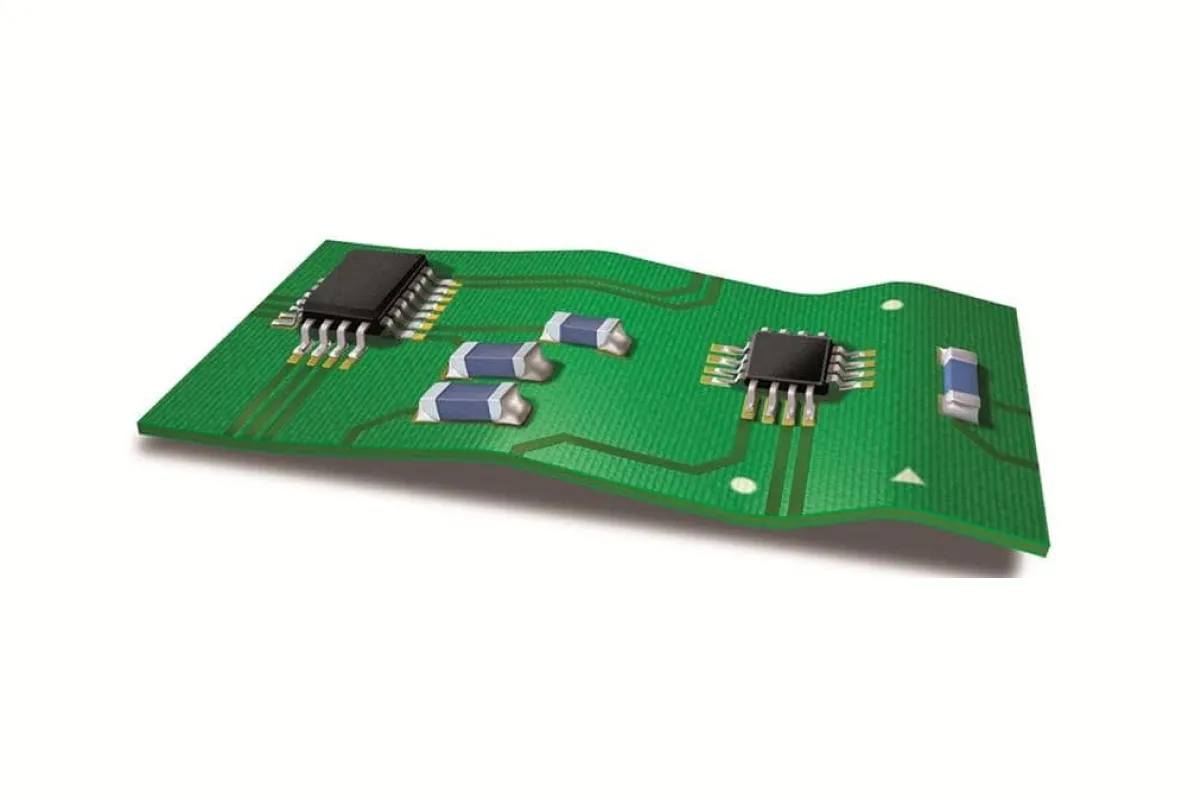
Printed Circuit Boards (PCBs) are the backbone of modern electronics, enabling everything from smartphones to aerospace systems. However, during manufacturing, large PCB panels can face a critical challenge: warpage. Warpage refers to the bending or deformation of a PCB panel, which can compromise component placement, solder joint reliability, and overall device performance. For engineers, controlling warpage in large PCB panels is essential to ensure high-quality, reliable products. In this blog, we explore the causes of PCB warpage, effective strategies to mitigate it, and best practices to maintain flatness during production.
Understanding PCB Warpage: Why It Happens
Warpage occurs when a PCB panel deviates from its intended flat shape due to thermal, mechanical, or material-related stresses during manufacturing. Large PCB panels, often used to optimize production efficiency, are particularly susceptible due to their size and the complex interplay of materials and processes. According to industry standards like IPC-6012, warpage is measured as a percentage of the board's length, with acceptable limits ranging from 0.05% for Class 4 (high-reliability applications) to 0.2% for Class 1 (general-purpose boards).
Key Causes of Warpage
Several factors contribute to warpage in large PCB panels:
- Thermal Stresses: During soldering or reflow processes, uneven heating and cooling create thermal gradients. For example, a temperature difference of 100°C across a panel can induce stresses that cause bending, especially in large panels exceeding 300 mm in length.
- Material Mismatches: The coefficient of thermal expansion (CTE) varies between materials like copper (17 ppm/°C) and FR-4 substrate (14-18 ppm/°C). This mismatch can cause differential expansion, leading to warpage.
- Copper Distribution Imbalance: Uneven copper distribution across layers can create asymmetrical stresses. For instance, a panel with 70% copper coverage on one side and 30% on the other is prone to twisting.
- Panel Design and Processing: Large panels often use V-cut dividers or chains in reflow furnaces, which can weaken structural integrity or unevenly distribute weight, increasing warpage risk.
- Thin Substrates: As demand grows for thinner PCBs (e.g., 0.8 mm or less), warpage becomes more pronounced due to reduced mechanical stability.
Suggested Reading:What Causes PCB Warpage?
The Impact of Warpage on PCB Performance
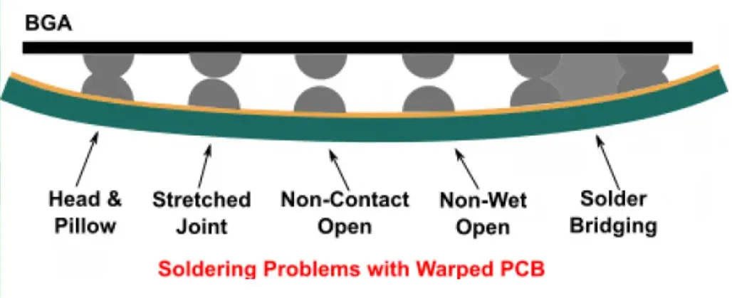
Warpage can significantly affect PCB functionality and reliability. For surface-mount technology (SMT) assembly, a flat PCB is critical for consistent component placement. If warpage exceeds 0.1% in high-reliability applications (Class 3 or 4), it can lead to:
- Solder Joint Failures: Uneven board height during reflow can cause solder bridging or open circuits, reducing joint reliability by up to 30% in severe cases.
- Component Misalignment: Pick-and-place machines require a constant height for accurate placement. PCB warpage can misalign components, leading to a 10-15% increase in assembly defects.
- Signal Integrity Issues: In high-frequency applications (e.g., signals >1 Gbps), warpage can distort trace geometry, increasing impedance mismatches by 5-10 ohms, which degrades performance.
- Mechanical Fit Issues: Warped panels may not fit properly in enclosures, causing assembly delays or device failures in industries like automotive or medical.
Strategies for Controlling Warpage in Large PCB Panels
To minimize warpage, engineers must address its root causes through careful design, material selection, and process optimization. Below are proven strategies to achieve flat, reliable PCB panels.
1. Optimize Material Selection
Choosing materials with compatible thermal and mechanical properties is critical. For large panels, consider:
- Low-CTE Substrates: Materials like high-Tg FR-4 (Tg >170°C) or polyimide (stable up to 260°C) reduce CTE mismatches with copper. These materials minimize thermal expansion differences by up to 20%.
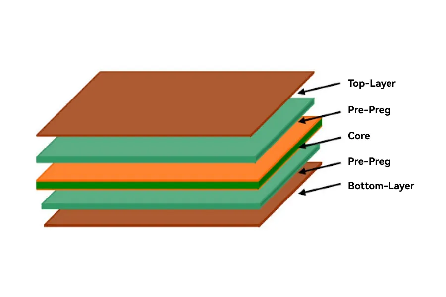
- Balanced Stackups: Ensure symmetrical layer stackups to distribute stresses evenly. For example, a 12-layer board with mirrored copper layers reduces warpage risk by 15-20% compared to asymmetrical designs.
- Core Thickness: Use thicker cores (e.g., 1.6 mm instead of 0.8 mm) for large panels to enhance rigidity, especially for panels over 400 mm.
2. Improve Copper Distribution
Balanced copper distribution across layers is essential to prevent asymmetrical stresses. Key practices include:
- Uniform Copper Coverage: Aim for 50-70% copper coverage on each layer. Use copper thieving (dummy patterns) to fill low-density areas, reducing warpage by up to 25%.
- Dummy Designs for BGAs: For Ball Grid Array (BGA) PCBs, implement bar-shaped dummy copper patterns near solder balls to stabilize the board, as demonstrated in studies reducing warpage by 10-15%.
- Avoid Large Copper Planes: Break large copper planes into smaller segments to minimize stress concentration. For example, segmenting a 100 mm² plane into four 25 mm² sections can reduce warpage by 5-10%.
3. Enhance Thermal Management
Proper PCB thermal management during manufacturing mitigates warpage caused by uneven heating. Effective techniques include:
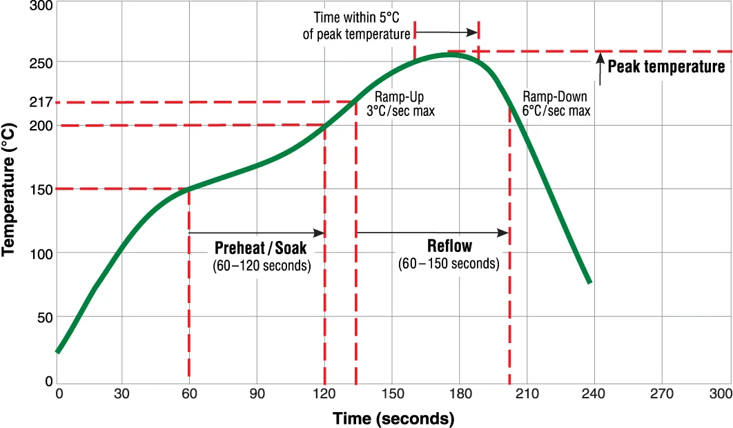
- Optimized Reflow Profiles: Use gradual heating and cooling rates (e.g., 1-2°C/s) to minimize thermal gradients. A well-tuned reflow profile can reduce warpage by 20-30%.
- Thermal Relief Features: Incorporate thermal relief pads in designs to dissipate heat evenly, particularly for high-power components. This can lower thermal stress by 15%.
- Uniform Furnace Design: Use reflow furnaces with consistent heat distribution to avoid hot spots. For large panels, ensure chains or supports are evenly spaced to prevent sagging.
4. Strengthen Panel Design
Panel design plays a significant role in warpage control. Consider these approaches:
- Stiffeners for Thin PCBs: Add metal stiffeners (e.g., aluminum or stainless steel) to coreless or thin BGA PCBs. Studies show stiffeners reduce warpage by up to 40% in flip-chip BGA designs.
- Minimize V-Cut Dividers: V-cuts weaken panel integrity. Limit their use or replace them with routed slots to maintain structural strength, reducing warpage risk by 10-15%.
- Panelization Techniques: Group PCBs on a panel with balanced spacing and support rails to distribute mechanical stress evenly. For example, a 500 mm x 400 mm panel with 10 mm rails can reduce warpage by 10%.
5. Implement Robust Testing and Inspection
Early detection of warpage ensures issues are addressed before assembly. Key testing methods include:
- In-Circuit Testing (ICT): Verifies electrical connectivity and detects warpage-related defects like open circuits. ICT can identify 90% of warpage-induced issues early in production.
- Test Coupons: Use test coupons with specific trace widths and impedance values (e.g., 50 ohms) to measure warpage. These coupons help identify deformation in critical areas, ensuring compliance with IPC standards.
- 3D Metrology: Employ laser-based 3D scanning to measure warpage with 0.01 mm precision. This is critical for large panels in high-reliability applications like aerospace.
Best Practices for Engineers
To effectively control warpage, engineers should adopt a holistic approach:
- Collaborate Early with Fabricators: Work with manufacturers during the design phase to align material choices and process parameters. This can reduce warpage issues by 20-30%.
- Simulate Designs: Use finite element analysis (FEA) tools to predict warpage based on material properties and thermal profiles. For example, FEA can identify stress points in a 12-layer board with 95% accuracy.
- Adhere to IPC Standards: Follow IPC-6012 guidelines for warpage limits (e.g., 0.1% for Class 3 boards) to ensure reliability in demanding applications.
- Iterate Prototypes: Test prototypes under real-world conditions to identify warpage risks before full-scale production. Rapid prototyping can catch 80% of potential issues early.
How ALLPCB Supports Warpage Control
At ALLPCB, we understand the challenges of managing warpage in large PCB panels. Our advanced manufacturing facilities and quick-turn prototyping services enable engineers to test and refine designs rapidly, minimizing warpage risks. With global logistics and precise process controls, we ensure uniform thermal profiles and high-quality materials, such as high-Tg FR-4 and polyimide, to meet stringent IPC standards. Our expert team collaborates with clients to optimize stackups and panelization, ensuring flat, reliable PCBs for applications from consumer electronics to aerospace.
Conclusion
Controlling warpage in large PCB panels is a complex but manageable challenge. By understanding the causes—thermal stresses, material mismatches, and design flaws—engineers can implement targeted strategies like balanced stackups, optimized reflow profiles, and robust testing. Adhering to industry standards and leveraging simulation tools further enhances reliability. At ALLPCB, we're committed to supporting engineers with cutting-edge manufacturing and rapid prototyping to deliver flat, high-performance PCBs. By applying these best practices, you can ensure your PCBs meet the demands of modern electronics with precision and reliability.


