 ALLPCB


In the fast-evolving world of electronics manufacturing, efficiency and cost-effectiveness are critical drivers of success. For engineers tasked with designing and producing printed circuit boards (PCBs), every decision impacts the bottom line—from material selection to assembly processes. One technique stands out as a game-changer in this space: PCB panelization. By grouping multiple individual PCBs onto a single larger panel, manufacturers can streamline production, reduce waste, and lower costs without compromising quality. But what exactly is panelization, and how can it transform your next project?
This blog dives deep into the world of PCB panelization, exploring its benefits, methods, and best practices. Whether you're working on a high-volume production run or a small batch of prototypes, understanding how to leverage panelization can save time, money, and resources. Let's unpack this essential manufacturing strategy and show you how to maximize its potential.
What Is PCB Panelization?
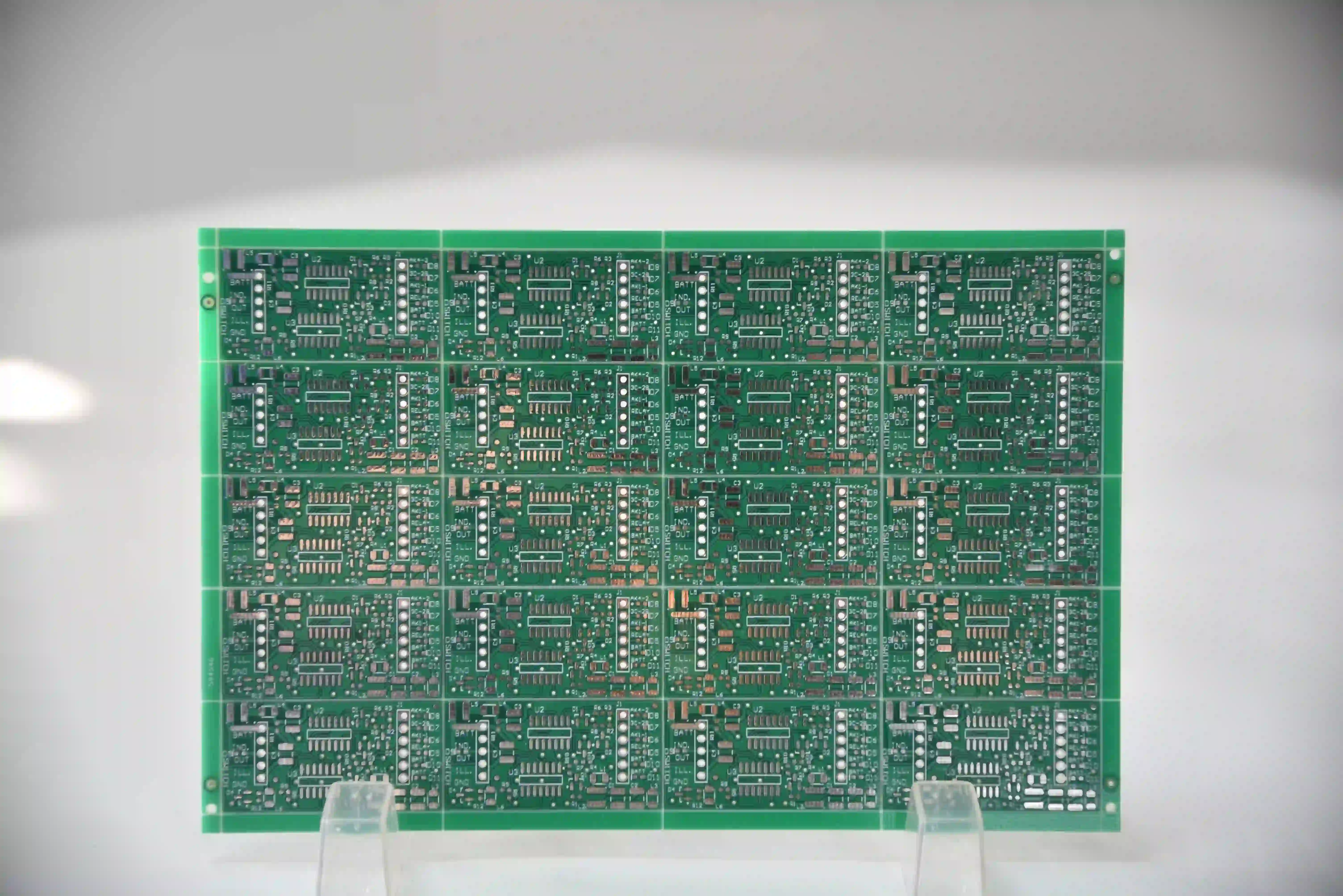
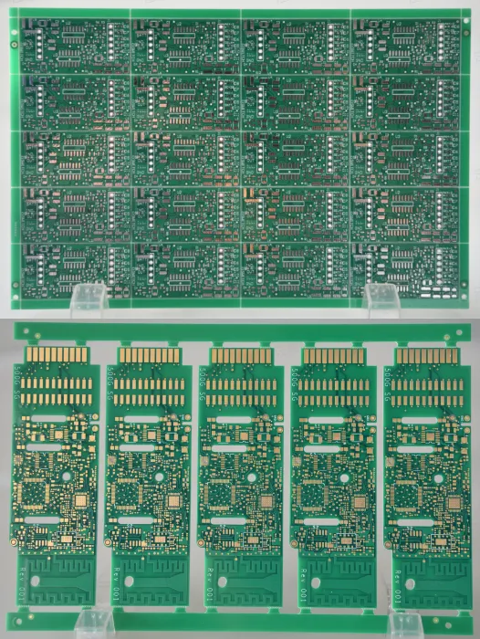
PCB panelization is the process of arranging multiple individual circuit boards onto a single, larger panel for manufacturing. Think of it as a way to batch-produce PCBs efficiently: instead of fabricating each board separately, we combine them into an array that moves through the assembly line as a single unit. Once assembly and testing are complete, the panel is separated—or depanelized—into individual boards ready for use.
This technique is especially valuable for small or irregularly shaped PCBs that are difficult to handle individually. For example, a board smaller than 50mm x 50mm might not fit standard conveyor systems in automated assembly lines. Panelization solves this by creating a larger, uniform structure that's easier to process. The result? Faster production, fewer errors, and optimized material use.
Why Panelization Matters in PCB Manufacturing
Engineers face constant pressure to deliver high-quality PCBs on time and within budget. Panelization addresses these challenges head-on by offering several key advantages:
1. Increased Production Efficiency
By processing multiple boards simultaneously, panelization reduces setup times and speeds up fabrication, assembly, and testing. For instance, a pick-and-place machine can populate components across an entire panel in one pass, rather than handling each board individually. This can cut assembly time by up to 50% in high-volume scenarios.
2. Cost Reduction
Material waste is a significant cost driver in PCB manufacturing. Panelization maximizes the use of standard laminate sizes—typically 18 x 24 inches or 21 x 24 inches—reducing scrap rates. In a study of high-volume production, optimized panel layouts increased board yield by 20%, translating to substantial savings per panel.
3. Improved Handling and Automation
Small boards are prone to damage or misalignment during manual handling. Panels provide structural stability, making them compatible with automated equipment like stencil printers and reflow ovens. This minimizes human error and ensures consistent quality across all boards.
4. Enhanced Quality Control
When boards are produced as a panel, they experience uniform conditions during fabrication and assembly. This consistency reduces variations—such as impedance mismatches or soldering defects—that might occur with individual processing. For example, maintaining a controlled impedance of 50 ohms across a panel is far easier than on standalone boards.
Suggested Reading:Mastering PCB Panelization: A Comprehensive Guide for Efficient Assembly
Common PCB Panelization Methods
Not all panelization techniques are created equal. The right method depends on your board design, production volume, and assembly requirements. Here are the most widely used approaches:
V-Scoring
V-scoring involves cutting V-shaped grooves into the panel's top and bottom surfaces along separation lines. Typically, each groove removes about one-third of the board thickness, leaving a thin "web" (e.g., 0.3mm) that holds the panel together until depanelization. After assembly, boards are snapped apart manually or with a simple tool.
- Pros: Cost-effective, no spacing required between boards, ideal for rectangular designs.
- Cons: Limited to straight edges; overhanging components near edges may get damaged.
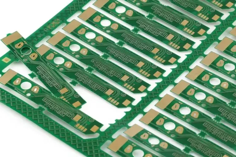
Tab Routing
Tab routing uses small, perforated tabs (often called "mouse bites") to connect individual boards to the panel. A CNC router cuts slots between boards, leaving these tabs intact until they're broken off post-assembly.
- Pros: Works with irregular shapes, accommodates edge-hanging components (e.g., USB connectors).
- Cons: Requires 2-3mm spacing between boards, increasing panel size and material costs.
Solid Tab Panelization
This method uses solid, unperforated tabs to connect boards, offering greater panel strength during assembly. Depanelization requires a router or saw to cut through the tabs.
- Pros: High stability for complex assemblies.
- Cons: More labor-intensive to separate, potential for rough edges.
Designing for Panelization: Key Considerations
To fully harness the benefits of panelization, engineers must design with manufacturing in mind. Here are critical factors to consider:
1. Board Layout and Spacing
Maximize the number of boards per panel while ensuring enough space for separation. For V-scoring, boards can be placed edge-to-edge, but tab routing requires at least 2mm clearance. A well-optimized layout might fit 20 small boards (e.g., 40mm x 40mm) on an 18 x 24-inch panel, compared to just 15 with poor planning.
2. Component Placement
Keep components at least 1-2mm from board edges to avoid damage during depanelization. For high-speed designs, ensure trace routing maintains signal integrity—e.g., a 50-ohm impedance trace should avoid sharp bends near panel edges.
3. Panel Strength
Add rails (typically 5-10mm wide) along the panel's edges to provide structural support and compatibility with conveyor systems. For large panels (e.g., 450mm x 330mm), include internal rails or additional tabs to prevent flexing during reflow soldering.
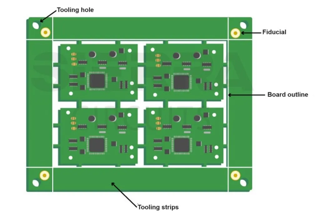
4. Fiducials and Tooling Holes
Incorporate fiducial marks—small copper targets (e.g., 1mm diameter)—in three corners of the panel for machine alignment. Add tooling holes (e.g., 2-3mm diameter) on rails to secure the panel during assembly. These features ensure placement accuracy within 0.01mm.
Benefits Beyond Efficiency: Real-World Examples
Panelization isn't just about speeding up production—it delivers tangible results across various scenarios. Let's explore a few examples:
High-Volume Production
A consumer electronics company producing 10,000 smartwatch PCBs (30mm x 30mm) switched from individual fabrication to panelization. By fitting 25 boards per 18 x 24-inch panel, they reduced material costs by 15% and cut assembly time from 10 minutes per board to 2 minutes per panel—a 75% improvement.
Small-Board Challenges
An IoT startup designing tiny sensor boards (20mm x 20mm) struggled with handling losses in their pick-and-place line. Panelizing 36 boards per panel with tab routing increased throughput by 40% and eliminated manual handling errors.
Prototyping Savings
A medical device engineer needed 50 prototype PCBs for testing. Panelizing five identical designs on a single panel reduced custom PCB cost from $10 per board to $6 per board, saving 40% while maintaining quality for impedance-sensitive circuits (e.g., 75 ohms).
Depanelization: The Final Step
Once PCB assembly is complete, separating the boards from the panel—PCB depanelization—is the final hurdle. The method depends on your panelization technique:
- V-Scoring: Boards are snapped apart by hand or with a pizza-cutter-like tool. Fast and simple, but edges may need cleaning if precision is critical.
- Tab Routing: Tabs are broken manually or cut with a router. Perforated tabs reduce stress on boards, keeping edge quality high.
- Routing/Sawing: For solid tabs or complex shapes, a CNC router or saw provides clean cuts, though it's slower and generates debris.
For high-reliability applications (e.g., aerospace), laser cutting offers unmatched precision, separating boards within 0.05mm tolerances. However, it's costlier and best reserved for niche cases.
Best Practices for Optimizing Panelization
To get the most out of panelization, follow these actionable tips:
1. Collaborate Early: Work with your manufacturer during the design phase to align panel specs with their equipment (e.g., max panel size of 450mm x 330mm).
2. Test Prototypes: Build a panelized prototype to identify issues like warping or component misalignment before scaling up.
3. Balance Cost and Yield: Avoid overpacking panels—leaving 5-10% unused space can prevent defects and reduce rework costs.
4. Use Software Tools: Leverage PCB design software (e.g., KiCad, Altium) with panelization features to simulate layouts and optimize board placement.
How ALLPCB Supports Your Panelization Needs
For engineers looking to implement panelization effectively, partnering with a reliable manufacturer is essential. At ALLPCB, we specialize in turning your designs into reality with advanced manufacturing capabilities and global logistics. Our quick-turn prototyping services let you test panelized designs in as little as 24 hours, while our expertise in high-volume production ensures cost-efficient scaling. Whether you need precise V-scoring for a dense array or tab routing for complex shapes, our team collaborates with you to optimize every panel, delivering high-quality PCBs that meet your exact specifications.
Conclusion: Unlocking the Power of Panelization
PCB panelization is more than a manufacturing trick—it's a strategic tool that maximizes efficiency, slashes costs, and boosts quality. By grouping boards into a single panel, engineers can streamline production, minimize waste, and tackle the challenges of small or high-volume designs. From V-scoring to tab routing, the right method depends on your project's unique needs, but the benefits are universal: faster turnarounds, lower expenses, and consistent results.
As you plan your next PCB project, consider how panelization can work for you. With thoughtful design and the right manufacturing partner, you'll unlock a world of efficiency that keeps your costs down and your quality up. Ready to get started? Dive into your design software, optimize that panel layout, and watch your production process transform.


