 ALLPCB


If you're looking to speed up your PCB development process, 3D printed PCB prototyping offers a game-changing solution for rapid iteration and testing. This guide dives deep into the world of 3D printed PCBs, covering everything from design basics to material choices and fast prototyping techniques. Whether you're an engineer, hobbyist, or innovator, you'll find actionable insights to streamline your workflow and bring ideas to life faster with 3D printing PCB materials and methods.
Introduction to 3D Printed PCB Prototyping
In the fast-paced world of electronics design, getting a working prototype quickly can make or break a project. Traditional PCB manufacturing often takes days or weeks, but 3D printed PCB prototyping cuts that time down significantly, sometimes to just hours. This innovative approach uses additive manufacturing to create functional circuit boards for testing and validation before full-scale production. By mastering rapid PCB prototyping with 3D printing, you can iterate designs faster, reduce costs, and stay ahead in competitive markets.
In this comprehensive 3D PCB design guide, we'll walk you through the essentials of 3D printed PCBs, including the tools, materials, and techniques needed for success. Let's explore how this technology is revolutionizing electronics prototyping.
What Are 3D Printed PCBs?
3D printed PCBs are circuit boards created using additive manufacturing technology instead of traditional subtractive methods like etching. In conventional PCB production, layers of copper are etched away from a substrate to form traces. In contrast, 3D printing builds the board layer by layer, depositing conductive materials for traces and insulating materials for the substrate. This allows for complex geometries and rapid production directly from digital designs.
The main advantage of 3D printed PCB prototyping is speed. You can go from a digital file to a testable board in a matter of hours, making it ideal for fast PCB iteration. Additionally, this method supports unique designs that might be challenging or costly with traditional manufacturing, such as curved or flexible circuits.
However, 3D printed PCBs are typically used for prototyping rather than final production. They may not yet match the performance of traditionally manufactured boards in terms of durability or signal integrity for high-frequency applications (e.g., above 1 GHz). Still, for initial testing and design validation, they are an invaluable tool.
Benefits of 3D Printed PCBs for Rapid Prototyping
Using 3D printing for rapid PCB prototyping offers several key advantages for engineers and designers. Here are the top benefits:
- Speed: Prototypes can be produced in hours rather than days or weeks. For example, a simple single-layer board might take just 2-4 hours to print.
- Cost-Effectiveness: Reduces expenses for small-batch prototypes by eliminating the need for expensive tooling or minimum order quantities.
- Design Flexibility: Allows for non-standard shapes and structures, such as embedding components within the board or creating 3D circuits.
- Fast Iteration: With quick turnaround times, you can test multiple design variations in a single day, accelerating the development cycle.
- Reduced Waste: Additive manufacturing only uses the material needed, minimizing scrap compared to subtractive methods.
These benefits make 3D printed PCB prototyping a powerful choice for anyone looking to innovate quickly in electronics design.
Key Steps in 3D Printed PCB Prototyping
Creating a 3D printed PCB involves several steps, from design to testing. Below is a detailed 3D PCB design guide to help you navigate the process for rapid prototyping.
1. Design Your PCB Layout
The first step is designing your circuit board using electronic design automation (EDA) software. Ensure your design is compatible with 3D printing by considering layer thickness, trace width, and material properties. Typical trace widths for 3D printed PCBs range from 0.2 to 0.5 mm, depending on the printer's resolution. Keep impedance in mind for signal integrity; for example, a 50-ohm impedance is standard for many RF applications, though achieving this with 3D printing may require calibration.
Export your design as a 3D model file (like STL) or in a format supported by your 3D printer software. Some tools allow direct integration with 3D printing workflows, simplifying this step.
2. Choose the Right 3D Printing Technology
Not all 3D printers are suitable for PCB prototyping. The two most common technologies for this purpose are:
- Fused Deposition Modeling (FDM): Uses thermoplastic filaments mixed with conductive materials for traces. It's affordable but less precise for fine traces.
- Inkjet or Aerosol Jet Printing: Deposits conductive inks onto a substrate with high precision, ideal for complex designs with trace widths as small as 0.1 mm.
Choose a printer based on your project's needs, balancing cost, precision, and material compatibility.
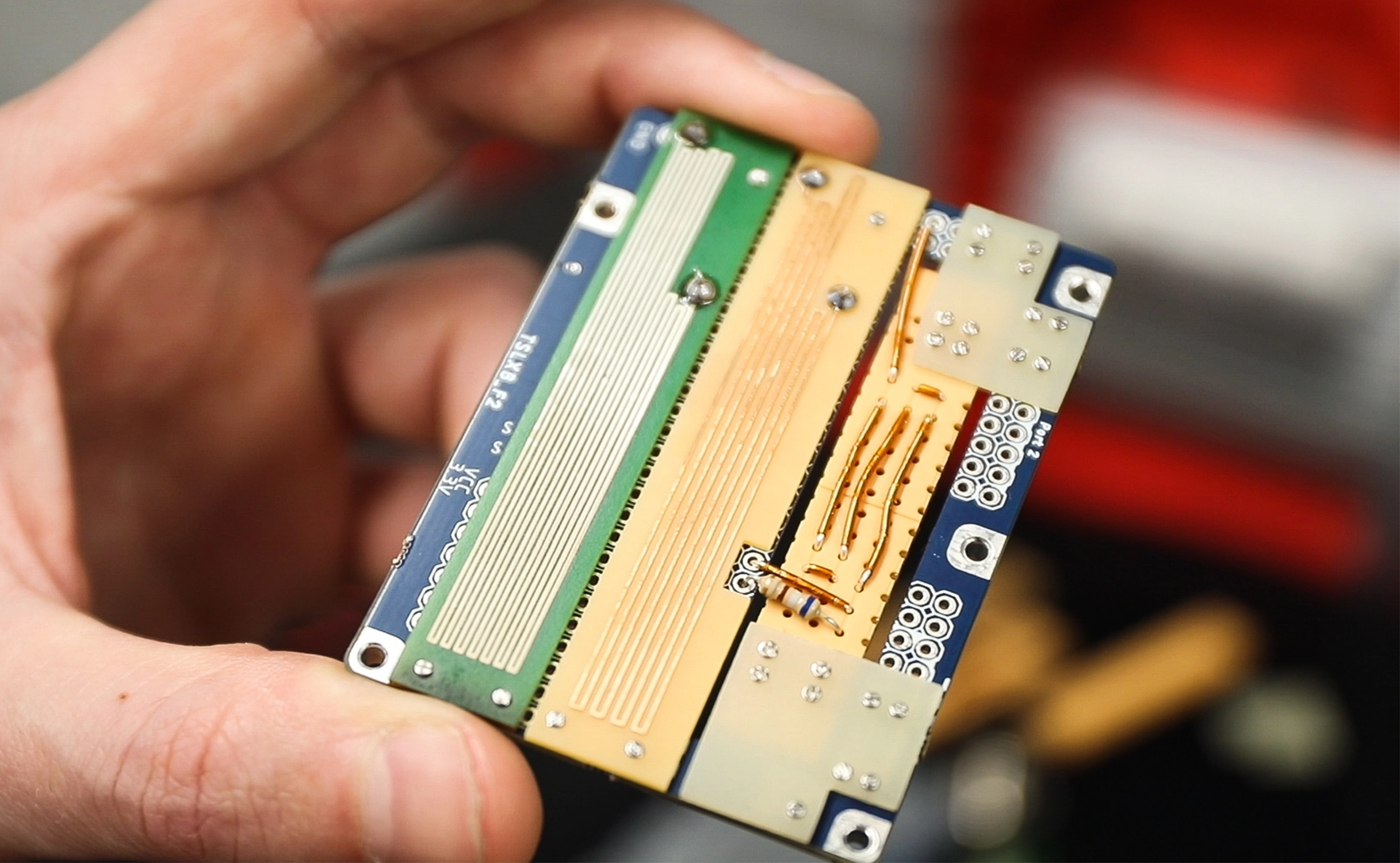
3. Select 3D Printing PCB Materials
Material selection is critical for 3D printed PCB prototyping. You'll need both insulating and conductive materials to create a functional board. Common choices include:
- Insulating Materials: PLA (polylactic acid) or ABS (acrylonitrile butadiene styrene) are often used for the substrate. These materials provide structural support and insulation between traces.
- Conductive Materials: Silver-based inks or graphene-infused filaments are popular for printing traces. Silver inks, for instance, offer resistivity as low as 1.6 x 10^-8 ohm-m, close to bulk silver, ensuring decent conductivity for low-power prototypes.
Keep in mind that material properties affect performance. For example, PLA substrates may degrade under high temperatures (above 60°C), so consider your operating environment when choosing 3D printing PCB materials.
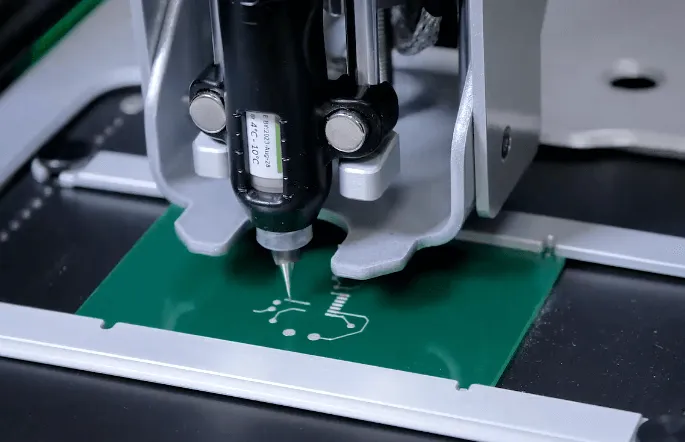
4. Print the PCB
Load your design into the 3D printer software and configure settings like layer height (typically 0.1-0.2 mm for PCBs) and print speed. Dual-material printers can alternate between insulating and conductive materials in a single print job, streamlining the process. Monitor the printing to avoid errors like misalignment of traces, which can lead to short circuits.
5. Post-Processing and Assembly
After printing, some boards require post-processing, such as curing conductive inks with heat or UV light to improve conductivity. Then, solder components onto the board if needed. Be cautious, as 3D printed substrates may not withstand high soldering temperatures (above 200°C for prolonged periods).
6. Test and Iterate
Test your prototype for functionality, checking for issues like open circuits or poor signal integrity. Use a multimeter to verify continuity and resistance across traces (aim for less than 1 ohm for short traces). If the design fails, tweak it in your software and print a new version. This fast PCB iteration cycle is where 3D printing truly shines.
Challenges and Limitations of 3D Printed PCBs
While 3D printed PCB prototyping offers incredible benefits, it’s not without challenges. Understanding these limitations helps set realistic expectations and plan accordingly.
- Material Performance: Conductive materials used in 3D printing often have higher resistance than copper (e.g., 10-100 times higher), which can affect performance in high-current or high-frequency applications above 100 MHz.
- Durability: Printed substrates may not handle mechanical stress or thermal cycling as well as FR-4, a common material in traditional PCBs, which can withstand temperatures up to 130°C.
- Precision: Achieving fine trace widths below 0.2 mm or consistent layer alignment can be difficult with some 3D printing technologies, leading to potential signal issues.
- Scalability: 3D printing is best for prototypes, not mass production. For large volumes, traditional manufacturing remains more cost-effective.
Despite these hurdles, ongoing advancements in materials and printing technology are closing the gap, making 3D printed PCBs more viable for a wider range of applications.
Tips for Successful 3D Printed PCB Prototyping
To maximize the benefits of rapid PCB prototyping with 3D printing, follow these practical tips:
- Start Simple: Begin with basic single-layer designs to familiarize yourself with the process before tackling multi-layer or complex boards.
- Calibrate Your Printer: Ensure precise alignment and material deposition by regularly calibrating your equipment. Misalignment by even 0.1 mm can cause shorts.
- Test Materials First: Experiment with small test prints to verify the conductivity and durability of your chosen 3D printing PCB materials before committing to a full design.
- Optimize for Signal Integrity: Design with wider traces (e.g., 0.5 mm) and shorter paths to minimize resistance and signal loss in prototypes.
- Document Iterations: Keep detailed notes on each design version and test outcome to track improvements and avoid repeating mistakes.
By following these strategies, you can achieve faster, more reliable results with your 3D printed PCB projects.
Future of 3D Printed PCBs in Rapid Prototyping
The field of 3D printed PCB prototyping is evolving rapidly, with exciting developments on the horizon. Researchers are working on new conductive materials with lower resistivity, closer to copper’s 1.68 x 10^-8 ohm-m, to improve performance. Additionally, hybrid manufacturing techniques that combine 3D printing with traditional methods are emerging, offering the best of both worlds for prototyping and production.
Another promising trend is the integration of embedded electronics during printing. Imagine printing a board with capacitors or resistors already inside, reducing assembly time and enabling more compact designs. As these technologies mature, 3D printed PCBs could become a staple not just for prototyping but also for small-batch production runs.
Conclusion: Accelerate Innovation with 3D Printed PCBs
Mastering 3D printed PCB prototyping opens up a world of possibilities for rapid PCB prototyping and fast PCB iteration. By leveraging the speed and flexibility of 3D printing, you can test ideas, refine designs, and bring products to market faster than ever before. From choosing the right 3D printing PCB materials to following a streamlined 3D PCB design guide, the process is accessible to engineers at all levels with the right tools and knowledge.
Start small, experiment with materials and designs, and embrace the iterative nature of this technology. With each prototype, you'll gain insights that push your projects forward. 3D printed PCBs are not just a trend—they're a powerful tool to drive innovation in electronics design. Dive in today and see how this approach can transform your workflow.


