 ALLPCB


If you're looking to optimize your printed circuit board (PCB) production process, mastering PCB panelization is key. PCB panelization is the practice of grouping multiple PCB designs onto a single panel for manufacturing and assembly, which boosts efficiency, reduces costs, and streamlines production. In this comprehensive guide, we'll walk you through everything you need to know about PCB panelization, from design rules and methods to tips for cost-effective practices and assembly efficiency.
Whether you're a beginner seeking a PCB panelization tutorial or an experienced engineer looking to refine your approach, this guide covers it all. Let's dive into the details of panelization design rules, compare different panelization methods, and explore how to achieve cost-effective panelization for your projects.
What Is PCB Panelization and Why Does It Matter?
PCB panelization is the process of arranging multiple individual PCB designs on a single larger panel. This panel is then used during manufacturing and assembly before the individual boards are separated, or "depanelized." The primary goal of panelization is to maximize efficiency during production by reducing material waste, simplifying handling, and speeding up assembly processes.
Why is this important? Without panelization, manufacturing individual small PCBs can be time-consuming and costly. By grouping several boards together, you minimize setup times for automated assembly machines, such as pick-and-place systems, and reduce the number of times materials need to be loaded and unloaded. For instance, assembling 100 small PCBs individually might take hours, whereas panelizing them into a single sheet can cut that time significantly—sometimes by as much as 50% depending on the setup.
Beyond efficiency, panelization also helps in maintaining consistency across boards, ensuring uniform soldering and component placement. This practice is especially critical for high-volume production where even small savings per board can add up to substantial cost reductions.
Key Benefits of PCB Panelization for Assembly Efficiency
Panelization offers several advantages that directly impact assembly efficiency. Here's a breakdown of the most significant benefits:
- Reduced Handling Time: Handling a single panel instead of dozens or hundreds of individual boards cuts down on manual labor and machine setup time. This is crucial for surface-mount technology (SMT) assembly lines where automation thrives on batch processing.
- Improved Component Placement Accuracy: Automated pick-and-place machines work more effectively on a larger, stable panel, reducing errors in component positioning. For high-density designs with components spaced as close as 0.5 mm, this precision is vital.
- Cost Savings: By optimizing the use of materials and minimizing waste, panelization lowers the per-unit cost. For example, using a panel size of 18 x 24 inches can often fit 20-30 small boards, maximizing the use of expensive substrate materials like FR-4.
- Faster Turnaround: Panelized boards move through manufacturing stages like etching, drilling, and testing more quickly since fewer individual setups are needed.
These benefits make panelization a cornerstone of modern PCB production, especially when striving for assembly efficiency in large-scale projects.
Panelization Design Rules: Best Practices for Success
Creating an effective panelization layout requires adhering to specific design rules to ensure manufacturability and ease of assembly. Below are essential guidelines to follow when designing your panel:
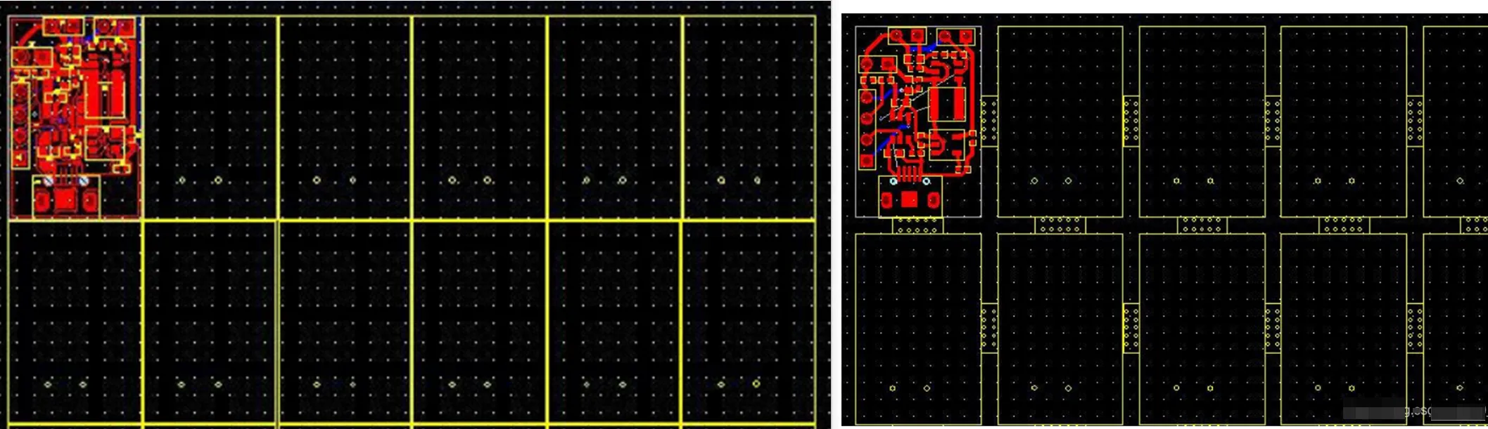
1. Panel Size and Material Utilization
Choose a panel size that maximizes the number of individual boards while fitting within standard manufacturing constraints, such as 18 x 24 inches or 12 x 18 inches. Leave at least 10-15 mm of border space around the edges for handling and tooling holes. This spacing prevents damage during production and ensures compatibility with assembly equipment.
2. Spacing Between Boards
Maintain adequate spacing between individual PCBs on the panel—typically 2-3 mm—to allow for clean separation during depanelization. Insufficient spacing can lead to damage, especially with delicate traces near board edges.
3. Tooling Holes and Fiducials
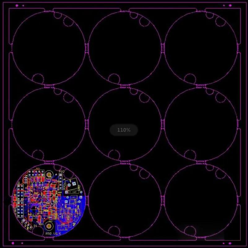
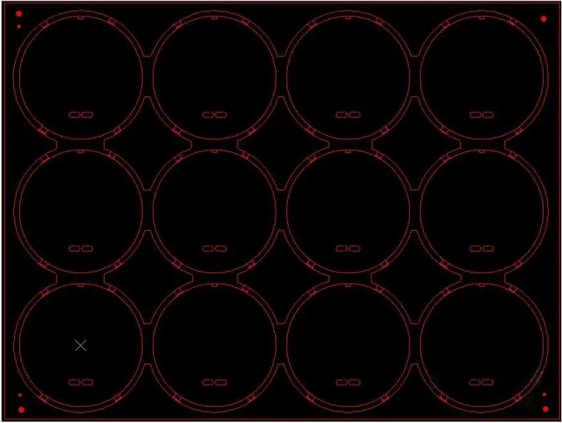
Include tooling holes (usually 3-4 mm in diameter) at the panel's corners for alignment during manufacturing. Additionally, place fiducial markers—small copper dots or crosses—near the corners of each individual board to help automated machines align components accurately. A common practice is to use three fiducials per board for optimal precision.
4. Breakaway Tabs or V-Cuts
Decide how the boards will be separated after assembly. Breakaway tabs (small perforated connections) or V-cuts (pre-scored lines) are common methods. Tabs should be 5-8 mm wide with 2-3 small holes (0.3 mm diameter) to weaken them for easy snapping. V-cuts, on the other hand, should align with the board edges and have a depth of about one-third of the board thickness (e.g., 0.5 mm for a 1.6 mm thick board).
5. Component Placement Near Edges
Avoid placing components too close to the board edges where separation occurs. A clearance of at least 3-5 mm ensures that components aren't damaged during depanelization, especially for sensitive parts like ceramic capacitors or fine-pitch ICs with lead spacing under 0.65 mm.
Panelization Methods Compared: Choosing the Right Approach
There are several methods to panelize PCBs, each with its own strengths and trade-offs. Let's compare the most common techniques to help you decide which suits your project best.
1. V-Cut Panelization
Overview: V-Cut panelization involves scoring V-shaped grooves along the separation lines using a specialized blade. This method is ideal for straight-edged boards.
Pros: Quick and cost-effective for high-volume production; clean separation with minimal stress on boards.
Cons: Limited to straight cuts, not suitable for irregular shapes; requires precise alignment to avoid damaging traces near edges.
Best For: Rectangular or square PCBs in bulk manufacturing.
2. Tab Routing (Breakaway Tabs)
Overview: Tab routing uses small connecting tabs with perforations to hold boards together. These tabs are broken manually or with tools after assembly.
Pros: Flexible for irregular shapes; allows for more complex panel designs.
Cons: Manual separation can be time-consuming and may leave rough edges; risk of stress on boards if tabs are too strong.
Best For: Small to medium runs with non-standard board shapes.
3. Mouse Bites
Overview: Similar to tab routing, mouse bites use a series of small drilled holes along the separation line to create a perforated connection.
Pros: Easy to separate by hand; works well for small boards.
Cons: Can leave rough edges; not ideal for high-density designs near separation lines.
Best For: Prototyping or low-volume projects with simple designs.
4. Mixed Methods
Overview: Some projects combine V-cuts and tabs to balance efficiency and flexibility, using V-cuts for straight edges and tabs for complex areas.
Pros: Offers versatility for mixed board shapes on the same panel.
Cons: Increases design complexity and manufacturing time.
Best For: Panels with varied board designs.
Cost-Effective Panelization: Balancing Design and Manufacturing Needs
Cost-effective panelization is all about finding the sweet spot between design complexity and manufacturing efficiency. Here are actionable tips to save on costs without sacrificing quality:
- Optimize Board Layout: Arrange boards to minimize wasted space on the panel. For example, rotating boards or nesting smaller designs within larger ones can increase the yield per panel, reducing material costs by up to 20% in some cases.
- Standardize Panel Sizes: Stick to industry-standard panel sizes to avoid custom fabrication fees. Using a common 18 x 24-inch panel can save 10-15% compared to non-standard dimensions.
- Choose the Right Separation Method: For high-volume runs, V-Cut panelization often costs less due to its speed and automation compatibility. For prototypes, mouse bites or tabs may be more economical since they don't require specialized scoring tools.
- Minimize Tooling Complexity: Limit the number of unique tooling holes or fiducial designs to reduce setup costs. Reusing standard configurations across projects can lower expenses by 5-10% per run.
- Collaborate Early with Manufacturers: Share your panelization design with your manufacturing partner during the planning stage. Their input on equipment capabilities and material constraints can prevent costly redesigns.
By focusing on these strategies, you can achieve cost-effective panelization that supports both your budget and production goals.
Common Challenges in PCB Panelization and How to Overcome Them
While panelization offers many benefits, it also comes with potential pitfalls. Here are some common challenges and solutions:
1. Board Damage During Depanelization
Issue: Improper separation methods or insufficient spacing can crack boards or damage components.
Solution: Use adequate spacing (2-3 mm) and test separation methods on a prototype panel. For delicate designs, consider using tab routing with weaker perforations to minimize stress.
2. Misalignment in Assembly
Issue: Inaccurate fiducials or tooling holes can lead to component placement errors, especially for fine-pitch parts with tolerances below 0.1 mm.
Solution: Double-check fiducial placement and ensure tooling holes match the manufacturer's specifications. Automated optical inspection (AOI) after assembly can catch misalignment early.
3. Material Waste
Issue: Poor layout planning can result in unused panel space, increasing costs.
Solution: Use software tools to simulate and optimize board arrangements before finalizing the design. Even a 5% improvement in material usage can lead to significant savings over thousands of units.
Tools and Software for PCB Panelization
Designing a panelized layout manually can be tedious and error-prone. Thankfully, modern design software offers built-in tools to simplify the process. Many electronic design automation (EDA) platforms include panelization features that allow you to arrange boards, add fiducials, and simulate separation methods. These tools often provide templates for standard panel sizes and generate manufacturing files with precise specifications.
Additionally, some manufacturers offer free online utilities to help with panelization during the quoting process. These tools can suggest optimal layouts based on your board dimensions and quantity, ensuring compatibility with their production equipment.
Final Thoughts on Mastering PCB Panelization
Mastering PCB panelization is a game-changer for anyone involved in electronics manufacturing. By understanding panelization design rules, comparing different methods, and focusing on assembly efficiency, you can significantly enhance your production process. Cost-effective panelization isn't just about cutting corners—it's about smart design choices that balance quality, speed, and budget.
Whether you're working on a small prototype run or a high-volume production, the principles outlined in this PCB panelization tutorial can guide you toward better outcomes. Start by optimizing your panel layout, adhering to best practices, and collaborating with your manufacturing partner to ensure seamless execution.
With these strategies in hand, you're well on your way to achieving efficient assembly and cost savings in your next PCB project. Keep refining your approach, and watch as panelization transforms your manufacturing workflow.


