 ALLPCB


When designing a printed circuit board (PCB), one of the most critical aspects to consider is the spacing between conductive elements, such as traces and pads. Trace-to-pad clearance, often referred to as the distance between a trace and a pad, plays a vital role in ensuring the reliability, safety, and performance of your PCB. In this comprehensive guide, we’ll dive deep into the essentials of trace-to-pad clearance, including minimum spacing guidelines, industry standards like IPC 2221, and practical tips for optimizing your PCB layout. Whether you’re a beginner or a seasoned engineer, this blog will equip you with the knowledge to design better PCBs.
At its core, trace-to-pad clearance is the minimum distance required between a conductive trace and a pad to prevent electrical issues like short circuits, arcing, or signal interference. This spacing depends on factors such as voltage levels, environmental conditions, and manufacturing capabilities. By adhering to proper guidelines, like those outlined in IPC 2221 standards, you can ensure your design is safe and functional. Let’s explore this topic in detail to help you master PCB clearance trace to pad requirements.
What Is Trace-to-Pad Clearance in PCB Design?
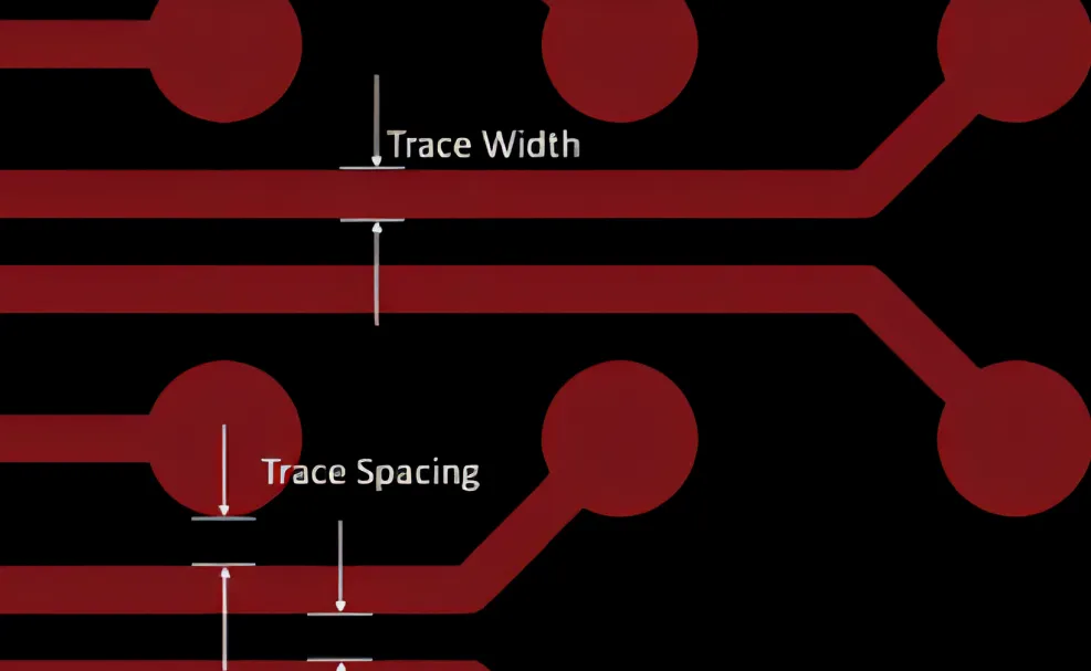
Trace-to-pad clearance refers to the physical distance between a conductive trace (a pathway for electrical signals on a PCB) and a pad (the metal area where components are soldered). This spacing is crucial because it prevents unintended electrical connections, reduces the risk of arcing in high-voltage designs, and minimizes crosstalk in high-speed circuits. Without proper clearance, your PCB could suffer from short circuits, reduced signal integrity, or even complete failure.
In practical terms, the trace-to-pad distance is influenced by the voltage difference between the trace and pad, the operating environment (like humidity or altitude), and the PCB’s intended application. For example, a low-voltage consumer device might require a clearance of just 0.2 mm, while a high-voltage industrial system could demand 2.5 mm or more to prevent arcing. Understanding and applying the correct minimum trace-to-pad spacing is a fundamental skill for any PCB designer.
Why Is Trace-to-Pad Clearance Important?
The importance of maintaining proper trace-to-pad spacing cannot be overstated. Here are the key reasons why this aspect of PCB design matters:
- Safety: In high-voltage designs, inadequate clearance can lead to electrical arcing, which poses a fire hazard or risk of component damage. Proper spacing ensures safety by preventing such issues.
- Signal Integrity: For high-speed digital circuits, close traces and pads can cause crosstalk, where signals interfere with each other, leading to data errors. Adequate clearance minimizes this interference.
- Manufacturability: PCB manufacturers have specific tolerances for spacing. If your trace-to-pad distance is too small, it may be difficult or impossible to fabricate, leading to production delays or defects.
- Reliability: Over time, environmental factors like dust, moisture, or thermal expansion can degrade a PCB. Proper clearance reduces the likelihood of short circuits or breakdowns under these conditions.
By prioritizing trace-to-pad clearance, you ensure that your PCB performs reliably throughout its lifespan, whether it’s powering a simple gadget or a complex industrial system.
Understanding IPC 2221 Trace Spacing Standards
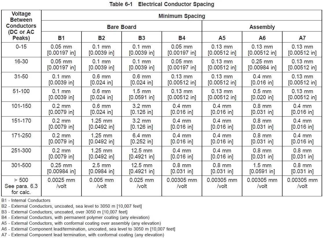
One of the most widely recognized standards for PCB design is IPC 2221, which provides guidelines for trace spacing and clearance based on voltage levels and environmental conditions. IPC 2221, titled "Generic Standard on Printed Board Design," offers a framework for determining safe distances between conductive elements, including trace-to-pad clearance, to prevent electrical breakdown.
According to IPC 2221, clearance requirements vary based on whether the conductors are on the same layer (external) or between layers (internal), and whether they are coated or uncoated. Here are some general guidelines from the standard for external conductors at sea level:
- For voltages up to 15V, a minimum clearance of 0.05 mm (2 mils) is recommended.
- For voltages between 15V and 30V, the clearance increases to 0.1 mm (4 mils).
- For voltages between 30V and 50V, a clearance of 0.6 mm (24 mils) is advised.
- For higher voltages, such as 100V to 150V, the clearance can go up to 1.5 mm (59 mils) or more, depending on the specific conditions.
These values are starting points and may need adjustment based on factors like altitude (air pressure affects arcing distance) or the presence of protective coatings. IPC 2221 also distinguishes between clearance (air gap) and creepage (surface distance along the board), both of which are critical for trace-to-pad spacing in high-voltage designs.
It’s worth noting that not all designs must strictly adhere to IPC 2221. Depending on your project’s requirements, you might need tighter or looser spacing. However, following these standards is a best practice for ensuring safety and reliability, especially for commercial or industrial applications.
Factors Affecting Minimum Trace-to-Pad Spacing
Several factors influence the minimum trace-to-pad spacing in a PCB design. Understanding these variables will help you determine the right clearance for your specific application.
1. Voltage Levels
The voltage difference between a trace and a pad is the primary factor in determining clearance. Higher voltages increase the risk of arcing, so larger distances are required. For instance, a design operating at 500V may need a clearance of 6 mm or more, while a 5V circuit might only require 0.2 mm.
2. Environmental Conditions
Humidity, temperature, and altitude can affect the dielectric strength of air and the PCB material. At high altitudes, where air pressure is lower, arcing occurs more easily, necessitating larger clearances. Similarly, high humidity can lead to condensation, increasing the risk of short circuits if spacing is too tight.
3. Signal Frequency and Speed
In high-speed designs, such as those with signal frequencies above 100 MHz, EMI compliance testing and crosstalk become significant concerns. Maintaining sufficient trace-to-pad distance helps reduce these effects, preserving signal integrity. For example, a high-speed USB signal might require a clearance of at least 0.3 mm to avoid interference with nearby pads.
4. Manufacturing Constraints
PCB fabrication processes have limits on how close traces and pads can be placed. Most standard manufacturing services can achieve clearances as low as 0.15 mm (6 mils), but tighter spacing may require advanced techniques or higher costs. Always consult your manufacturer’s design rules to ensure your trace-to-pad distance is achievable.
5. Board Material and Coating
The type of PCB material (e.g., FR-4) and any protective coatings or solder masks can influence clearance requirements. A coated board might allow for slightly reduced spacing since the coating adds an extra layer of insulation, but uncoated boards typically require more conservative distances.
Suggested Reading:Mastering Trace-to-Pad Spacing for Optimal Signal Integrity
How to Determine the Right Trace-to-Pad Distance
Calculating the optimal trace-to-pad distance for your PCB involves balancing safety, performance, and manufacturability. Here’s a step-by-step approach to ensure you get it right:
- Identify Voltage Levels: Determine the maximum voltage difference between the trace and pad. Use this value to reference IPC 2221 clearance guidelines or other relevant standards.
- Assess Environmental Factors: Consider the operating environment of your PCB. If it will be used in a humid or high-altitude setting, increase the clearance beyond the baseline recommendations.
- Check Signal Requirements: For high-speed or high-frequency signals, ensure the clearance is sufficient to prevent crosstalk or EMI. Simulation tools can help model these effects if needed.
- Review Manufacturer Guidelines: Confirm the minimum trace-to-pad spacing supported by your PCB manufacturer. Adjust your design if necessary to meet their capabilities.
- Use Design Software Rules: Most PCB design software allows you to set clearance rules based on net classes or specific components. Configure these rules to enforce the desired trace-to-pad distance during layout.
By following these steps, you can ensure that your design adheres to best practices for PCB clearance trace to pad requirements while meeting the unique needs of your project.
Common Mistakes in Trace-to-Pad Clearance Design
Even experienced designers can make errors when it comes to trace-to-pad spacing. Here are some common pitfalls to avoid:
- Ignoring Voltage Ratings: Underestimating the voltage difference between a trace and pad can lead to insufficient clearance, increasing the risk of arcing or short circuits.
- Overlooking Creepage: Clearance (air gap) is important, but creepage (surface distance) is equally critical, especially in humid environments where surface contamination can cause shorts.
- Neglecting High-Speed Effects: Failing to account for crosstalk in high-speed designs can degrade signal quality, even if voltage-based clearance is adequate.
- Exceeding Manufacturing Limits: Designing with clearances smaller than what your manufacturer can produce often results in costly redesigns or production issues.
Avoiding these mistakes will save you time and resources while ensuring your PCB performs as intended.
Practical Tips for Optimizing Trace-to-Pad Clearance
Designing a PCB with proper trace-to-pad spacing doesn’t have to be complicated. Here are some actionable tips to help you optimize your layout:
- Use Design Rule Checks (DRC): Leverage the DRC features in your PCB design software to automatically flag clearance violations during the layout process.
- Group Similar Nets: Place traces and pads with similar voltage levels or signal types closer together to minimize the need for large clearances across the board.
- Prioritize High-Voltage Areas: Identify and isolate high-voltage sections of your PCB early in the design process, ensuring they have ample clearance from low-voltage areas.
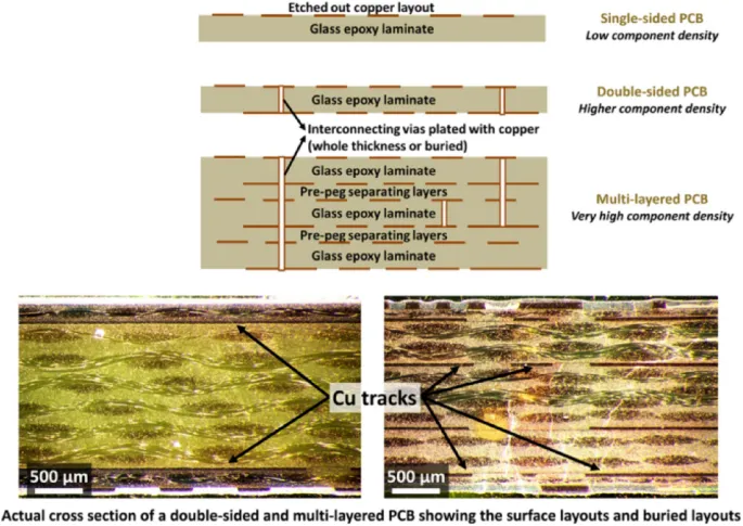
- Consider Multi-Layer Boards: If space is tight on a single-layer PCB, use multiple layers to separate high-voltage or high-speed traces and pads, reducing clearance concerns.
- Test and Validate: After completing your design, simulate or prototype the PCB to verify that the trace-to-pad distance performs as expected under real-world conditions.
These strategies will help you create a robust PCB layout that balances clearance requirements with design efficiency.
Conclusion: Mastering Trace-to-Pad Clearance for Better PCBs
Trace-to-pad clearance is a fundamental aspect of PCB design that directly impacts safety, performance, and manufacturability. By understanding the importance of trace-to-pad distance, adhering to industry standards like IPC 2221 trace spacing guidelines, and considering factors such as voltage, environment, and signal speed, you can create reliable and efficient PCB layouts. Avoiding common mistakes and applying practical optimization tips further ensures that your design meets the highest standards of quality.
Whether you’re working on a low-voltage consumer device or a high-voltage industrial system, mastering minimum trace-to-pad spacing is essential for success. With the insights and strategies shared in this guide, you’re well-equipped to tackle PCB clearance challenges and deliver designs that stand the test of time. Keep these principles in mind during your next project, and you’ll see the difference that proper spacing can make.


