


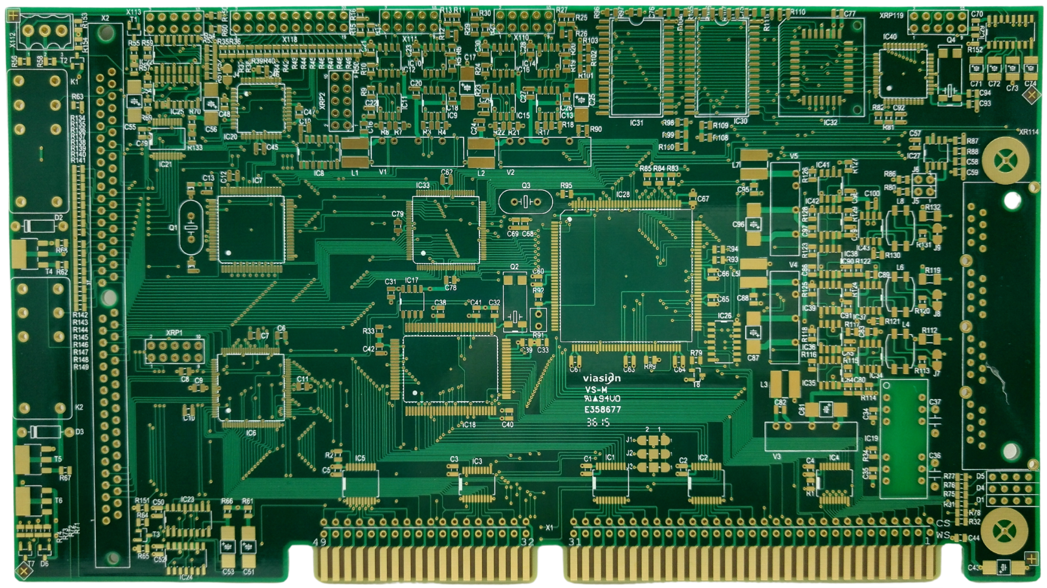
In the world of printed circuit board (PCB) design, achieving optimal signal integrity is crucial for ensuring reliable performance, especially in high-frequency applications. One often overlooked aspect that plays a significant role in maintaining signal quality is trace-to-pad spacing. So, how does trace-to-pad spacing impact signal integrity, and what are the best practices for managing it? Simply put, proper spacing between traces and pads helps minimize signal reflection, crosstalk, and impedance mismatches, ensuring clean signal transmission across your PCB.
In this comprehensive guide, we'll dive deep into the importance of trace-to-pad spacing for PCB signal integrity, explore how it relates to signal reflection and impedance control, and provide actionable tips for high-frequency designs. Whether you're a seasoned engineer or just starting out, this post will equip you with the knowledge to optimize your layouts for peak performance.
Why Trace-to-Pad Spacing Matters for Signal Integrity
Signal integrity refers to the ability of a signal to travel from its source to its destination without distortion or loss. In PCB design, factors like trace width, length, and spacing all influence how signals behave. Trace-to-pad spacing, in particular, is critical because it affects the electromagnetic fields around a signal path. If the spacing is too tight or inconsistent, it can lead to issues like crosstalk, signal reflection, and impedance mismatches—problems that degrade performance, especially at high frequencies.
For instance, in a high-speed digital circuit operating at 5 GHz, improper spacing between a trace and a nearby pad can cause unwanted coupling, leading to noise that interferes with data transmission. By carefully controlling trace-to-pad spacing, you can reduce these risks and maintain the integrity of your signals.
Understanding Signal Reflection in Trace-to-Pad Design
Signal reflection occurs when a signal encounters a change in impedance along its path, causing part of the signal to bounce back toward the source. This can happen at the junction between a trace and a pad if the transition isn't designed properly. Reflections distort the signal, leading to errors in data transmission, especially in high-frequency circuits where timing is critical.
The key to minimizing signal reflection in trace-to-pad transitions is maintaining consistent impedance. Impedance is influenced by the geometry of the trace, the dielectric material of the PCB, and the spacing between conductive elements. For example, a trace with a width of 10 mils on a standard FR-4 substrate might have a characteristic impedance of 50 ohms. If the pad connected to this trace disrupts that impedance due to poor spacing or size, reflections will occur.
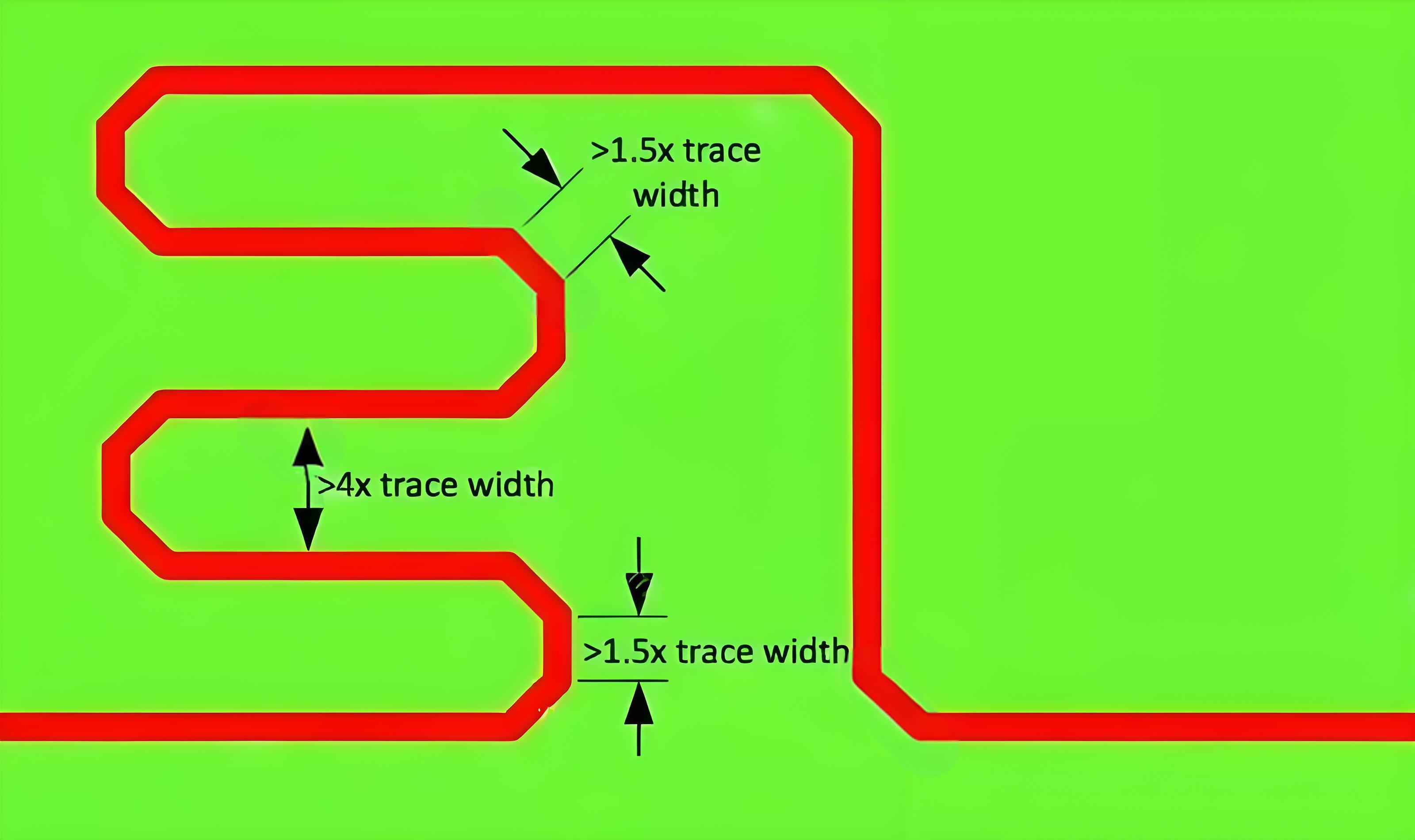
To avoid this, ensure that the pad size and shape are optimized for the trace width, and maintain adequate spacing to prevent abrupt changes in the signal path. A common rule of thumb is to keep the pad width no more than 1.5 times the trace width to minimize impedance discontinuity.
Impedance Control and Trace Spacing in PCB Design
Impedance control is a cornerstone of high-frequency PCB design, and trace-to-pad spacing plays a vital role in achieving it. Characteristic impedance is the resistance a signal encounters as it travels along a trace, and any mismatch can cause reflections or signal loss. For high-speed signals, such as those in USB 3.0 or HDMI interfaces, maintaining a consistent impedance (often 50 ohms or 90 ohms for differential pairs) is non-negotiable.
Trace-to-pad spacing impacts impedance by altering the electromagnetic field distribution around the signal path. If a trace is too close to a pad, the capacitance between them increases, lowering the impedance at that point. This mismatch can degrade signal quality. A practical guideline for impedance control is to maintain a spacing of at least 3 times the trace width between the trace and any adjacent pad or conductor, though this can vary based on the dielectric constant of your board material and the target impedance.
For example, in a 4-layer PCB with a signal layer and a ground plane, a trace width of 8 mils might require a spacing of 24 mils from nearby pads to maintain a 50-ohm impedance. Tools like impedance calculators or simulation software can help you fine-tune these values for your specific design.
Trace-to-Pad Spacing in High-Frequency Applications
High-frequency designs, such as those for RF circuits or high-speed digital systems, are particularly sensitive to trace-to-pad spacing. At frequencies above 1 GHz, even small variations in spacing can lead to significant signal degradation due to parasitic capacitance and inductance. For instance, in an RF circuit operating at 2.4 GHz, a spacing error of just a few mils between a trace and a pad can introduce enough capacitance to detune the circuit.
To optimize trace-to-pad spacing for high-frequency applications, consider the following best practices:
- Avoid Overlapping Pads: Ensure pads are not unnecessarily large or positioned too close to traces, as this increases parasitic effects.
- Use Ground Planes: Place a solid ground plane beneath high-frequency traces to stabilize impedance and reduce interference. Keep spacing consistent to avoid disrupting the return path.
- Minimize Via Usage Near Pads: Vias near pads can introduce inductance, so route traces carefully to avoid unnecessary transitions.
Additionally, consider the dielectric material of your PCB. High-frequency designs often benefit from low-loss materials with a dielectric constant (Dk) between 3.0 and 4.0, as they help maintain signal integrity over long traces. Adjust spacing based on the material’s properties to achieve the desired impedance.
Practical Tips for Optimizing Trace-to-Pad Spacing
Now that we've covered the theory behind trace-to-pad spacing for PCB signal integrity, let's explore some actionable tips to implement in your designs. These strategies will help you tackle signal reflection, impedance control, and high-frequency challenges effectively.
1. Calculate Spacing Based on Trace Width
A general rule for trace-to-pad spacing is to keep it at least 3 times the width of the trace. For a 10-mil trace, aim for a 30-mil gap to minimize coupling and maintain impedance. Adjust this based on your design's frequency and impedance requirements.
2. Use Design Software for Simulations
Modern PCB design tools often include simulation features to model signal behavior and impedance. Run simulations to test different trace-to-pad spacing configurations before finalizing your layout. This can save time and prevent costly revisions.
3. Pay Attention to Pad Geometry
The shape and size of pads influence signal transitions. Use rounded or teardrop-shaped pads for high-speed traces to reduce sharp corners that can cause reflections. Keep pad dimensions proportional to trace width for smoother signal flow.
4. Route Traces Away from High-Density Pad Areas
In densely populated boards, it's tempting to route traces close to pads to save space. However, this increases the risk of crosstalk. Plan your layout to prioritize spacing, even if it means using additional layers or rerouting traces.
5. Test and Iterate
After completing your design, prototype the board and test for signal integrity issues using tools like oscilloscopes or network analyzers. Measure parameters like return loss and eye diagrams to identify any problems caused by trace-to-pad spacing, then adjust as needed.
Common Mistakes to Avoid with Trace-to-Pad Spacing
Even experienced designers can make errors when it comes to trace-to-pad spacing. Here are some common pitfalls to watch out for in your PCB layouts:
- Ignoring Spacing in Dense Designs: Sacrificing spacing to fit more components can lead to crosstalk and signal degradation. Always prioritize signal integrity over board density.
- Overlooking Ground Plane Voids: Voids or cuts in the ground plane near pads can disrupt return paths, causing impedance mismatches. Ensure a continuous ground plane beneath critical signals.
- Using Default Pad Sizes: Default pad sizes in design software may not suit high-frequency traces. Customize pad dimensions to match your trace width and impedance goals.
- Neglecting Frequency Effects: Spacing rules for low-frequency designs don't apply to high-frequency circuits. Always scale your spacing considerations based on the operating frequency of your signals.
By being mindful of these mistakes, you can avoid unnecessary redesigns and ensure your PCB performs as intended.
The Role of Materials and Manufacturing in Trace-to-Pad Spacing
Beyond design techniques, the materials and manufacturing processes used in PCB fabrication also influence trace-to-pad spacing and signal integrity. The dielectric constant (Dk) and dissipation factor (Df) of your board material affect how signals propagate and how much spacing is needed to control impedance. For example, FR-4, a common PCB material, has a Dk of about 4.5, which works for many applications but may introduce losses at frequencies above 1 GHz. For such cases, consider advanced materials like Rogers laminates with a lower Dk for better performance.
Manufacturing tolerances also matter. If a fabricator cannot achieve tight control over trace widths or spacing, your carefully calculated design may not translate to the final product. Partner with a reliable manufacturer who can meet your specifications, especially for high-frequency or impedance-controlled designs. Specify your trace-to-pad spacing requirements clearly in your design files to avoid discrepancies during production.
Conclusion: Elevate Your PCB Designs with Proper Trace-to-Pad Spacing
Mastering trace-to-pad spacing is a fundamental step toward achieving optimal signal integrity in your PCB designs. By understanding how spacing impacts signal reflection, impedance control, and high-frequency performance, you can create layouts that deliver reliable, high-quality signal transmission. From calculating appropriate spacing based on trace width to selecting the right materials and avoiding common mistakes, every detail counts in ensuring your design meets its performance goals.
As you apply these principles to your next project, remember that small adjustments in trace-to-pad spacing can make a big difference in the overall functionality of your board. With careful planning, simulation, and testing, you'll be well on your way to designing PCBs that excel in even the most demanding applications. Focus on precision, and let signal integrity be the foundation of your success.