 ALLPCB


In the fast-evolving world of industrial control systems, the demand for smaller, faster, and more efficient electronics is at an all-time high. High-Density Interconnect (HDI) PCBs have emerged as a game-changer, enabling miniaturization without sacrificing performance. If you're wondering how HDI PCB design, microvias, fine-pitch components, miniaturization techniques, and high-layer count PCBs can transform industrial control applications, you're in the right place. This blog dives deep into the world of HDI technology, offering practical insights and detailed explanations tailored for engineers and designers.
What Are HDI PCBs and Why Do They Matter for Industrial Control?
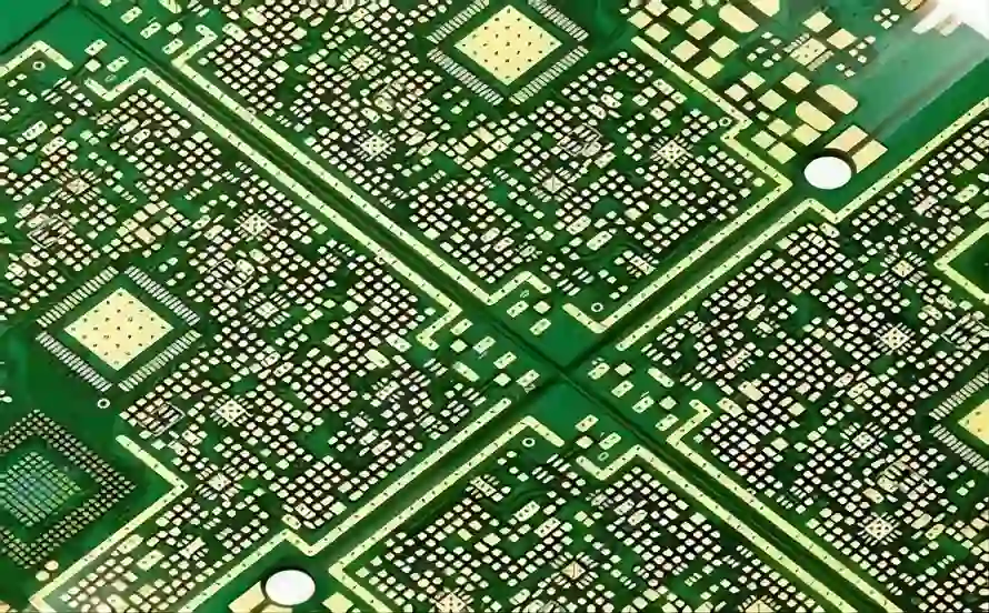
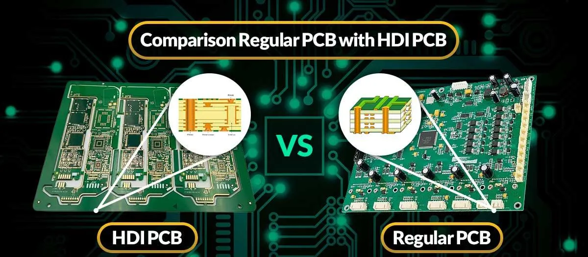
High-Density Interconnect (HDI) PCBs are advanced printed circuit boards designed to pack more components into a smaller space. Unlike traditional PCBs, HDI boards feature finer lines, smaller vias, and higher layer counts, allowing for greater wiring density per unit area. This makes them ideal for industrial control systems where space is often limited, and reliability is non-negotiable.
In industrial settings, equipment like programmable logic controllers (PLCs), sensors, and human-machine interfaces (HMIs) must operate flawlessly under harsh conditions. HDI PCBs support these devices by enabling compact designs, reducing signal delays, and improving thermal management. With the ability to handle complex circuitry in a smaller footprint, HDI technology is driving innovation in automation and control systems.
The Core Elements of HDI PCB Design
Creating an effective HDI PCB for industrial control requires careful attention to several key elements. Let’s break down the critical aspects of HDI PCB design that ensure performance and reliability.
1. Microvias: The Backbone of Miniaturization
Microvias are tiny holes, typically less than 150 micrometers in diameter, used to connect different layers of an HDI PCB. Unlike traditional through-hole vias, microvias are drilled using laser technology, allowing for precise placement and smaller sizes. This results in higher routing density and more space for components.
In industrial control applications, microvias play a vital role in reducing board size while maintaining signal integrity. For instance, a typical HDI board might use microvias with an aspect ratio of 0.75:1, ensuring reliable interlayer connections without compromising structural stability. By minimizing the space needed for vias, designers can fit more circuitry into compact modules like motor control units.
2. Fine-Pitch Components for Greater Density
Fine-pitch components refer to parts with closely spaced leads or pins, often less than 0.5 mm apart. These components are essential for HDI designs because they allow more functionality to be packed into a smaller area. In industrial control, fine-pitch components are commonly used in microcontrollers and sensor interfaces, where every millimeter of space counts.
However, working with fine-pitch components requires precise manufacturing and assembly processes. The alignment must be accurate to within 0.1 mm to avoid soldering defects or signal interference. Advanced HDI PCB design tools help engineers optimize layouts for fine-pitch components, ensuring reliable performance even in high-vibration environments like factory floors.
3. Miniaturization Techniques in Action
Miniaturization techniques are at the heart of HDI PCB innovation. These methods focus on reducing the size of the board while maintaining or even enhancing its capabilities. Some common miniaturization techniques include:
- Stacked Vias: Layering microvias on top of each other to connect multiple layers without increasing board size.
- Blind and Buried Vias: Using vias that don’t pass through the entire board to save space and improve routing efficiency.
- Thin Dielectrics: Employing materials with a thickness of less than 100 micrometers to reduce the overall height of the PCB stack-up.
In industrial control, miniaturization techniques enable the creation of compact devices like IoT-enabled sensors. For example, a sensor module for monitoring machine temperature might use an HDI PCB with blind vias to fit within a 20 mm x 20 mm footprint, allowing seamless integration into tight spaces.
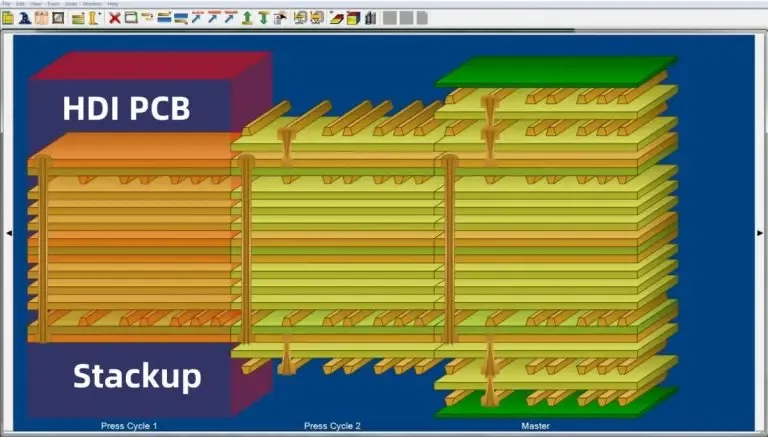
4. High-Layer Count PCBs for Complex Systems
High-layer count PCBs, often exceeding 10 layers, are a hallmark of HDI technology. These boards accommodate complex circuitry by stacking multiple layers of conductive traces and insulating materials. In industrial control, high-layer count PCBs are essential for applications requiring numerous input/output connections, such as robotic control systems.
A typical high-layer count HDI PCB might feature 12 to 20 layers, with each layer having a thickness of around 0.1 mm. This allows for intricate routing while keeping impedance values stable, often within a range of 50 to 100 ohms for high-speed signals. The result is a board that can handle data transfer rates of up to 10 Gbps, crucial for real-time control in industrial automation.
Benefits of HDI PCBs in Industrial Control Applications
HDI PCBs offer several advantages that make them indispensable for industrial control systems. Here’s how they stand out in demanding environments.
Enhanced Reliability in Harsh Conditions
Industrial control equipment often operates in extreme temperatures, high humidity, and constant vibration. HDI PCBs are designed to withstand these challenges through robust materials and precise manufacturing. For instance, using high-Tg (glass transition temperature) materials with values above 170°C ensures the board remains stable even at elevated temperatures.
Additionally, the smaller size of HDI boards reduces the risk of mechanical stress points, improving durability. This reliability is critical for applications like conveyor belt controllers, where downtime can cost thousands of dollars per hour.
Improved Signal Integrity for High-Speed Data
Signal integrity is a top priority in industrial control, where delays or interference can lead to system failures. HDI PCBs minimize signal loss by using shorter trace lengths and controlled impedance designs. For example, a well-designed HDI board can maintain signal speeds of up to 5 GHz with minimal crosstalk, ensuring accurate data transmission in real-time monitoring systems.
Space Savings for Compact Designs
Space constraints are a common challenge in industrial control panels, where multiple devices must fit into limited enclosures. HDI PCBs address this by reducing board size by up to 40% compared to traditional designs. This allows engineers to create smaller, lighter equipment without compromising functionality, ideal for portable diagnostic tools or embedded systems.
Challenges in HDI PCB Design and How to Overcome Them
While HDI PCBs offer incredible benefits, they also come with unique challenges. Understanding these hurdles and their solutions can help engineers achieve optimal results.
Complex Manufacturing Requirements
HDI PCB production involves advanced techniques like laser drilling for microvias and sequential lamination for high-layer count designs. These processes demand precision and can increase costs. To manage this, designers should collaborate closely with manufacturing teams during the early stages to ensure the design aligns with production capabilities.
Thermal Management Issues
With components packed tightly together, heat dissipation becomes a concern. Overheating can degrade performance or damage the board. To address this, engineers can incorporate thermal vias and heat sinks into the design. For example, placing thermal vias near high-power components can reduce temperatures by up to 15°C, extending the lifespan of the PCB.
Signal Interference in High-Density Layouts
The close proximity of traces and components in HDI designs can lead to electromagnetic interference (EMI). To mitigate this, designers should use ground planes between signal layers and maintain a minimum spacing of 0.2 mm between high-speed traces. These practices help keep EMI levels below acceptable thresholds, ensuring consistent performance.
Practical Tips for Designing HDI PCBs for Industrial Control
For engineers looking to leverage HDI technology in industrial control projects, here are some actionable tips to guide the design process.
- Start with a Clear Stack-Up Plan: Define the number of layers and via types early in the design phase to avoid routing issues later. A 16-layer stack-up with alternating signal and ground planes can optimize performance.
- Prioritize Component Placement: Position fine-pitch components strategically to minimize trace lengths and reduce signal delays. Use design software to simulate placement before finalizing the layout.
- Test for Signal Integrity: Use simulation tools to analyze impedance and crosstalk. Aim for a target impedance of 50 ohms for differential pairs to ensure reliable high-speed data transfer.
- Choose the Right Materials: Opt for low-loss dielectrics with a dielectric constant (Dk) of 3.5 or lower to support high-frequency signals without excessive attenuation.
Future Trends: HDI PCBs in Industrial Control
The future of HDI PCBs in industrial control looks promising, with several trends shaping their evolution. The rise of Industry 4.0 is driving demand for smarter, more connected systems, and HDI technology is at the forefront of this transformation. Innovations like embedded components, where passive elements are integrated directly into the PCB, are set to further reduce size and improve efficiency.
Additionally, advancements in materials science are leading to substrates with even lower dielectric constants, supporting signal speeds beyond 10 GHz. As industrial control systems become more reliant on IoT and AI, HDI PCBs will play a crucial role in enabling compact, high-performance solutions.
Conclusion: Embracing HDI for Industrial Innovation
High-Density Interconnect (HDI) PCBs are revolutionizing industrial control by offering unparalleled miniaturization and performance. From microvias and fine-pitch components to high-layer count designs, HDI technology provides the tools needed to create compact, reliable systems for the most demanding applications. By understanding the intricacies of HDI PCB design and applying miniaturization techniques, engineers can push the boundaries of what’s possible in industrial automation.
Whether you're designing a sensor for a smart factory or a controller for heavy machinery, HDI PCBs offer the flexibility and efficiency to meet modern challenges. With the right approach, these miniaturization marvels can help you achieve smaller, smarter, and more powerful solutions for industrial control.


