If you're wondering about the best silkscreen DPI for PCB designs, the ideal resolution typically ranges between 300 and 600 DPI for most manufacturing processes. This range ensures clear, legible markings without overloading the printing equipment or increasing costs unnecessarily. But there's more to it than just picking a number. In this comprehensive guide, we'll dive deep into silkscreen DPI for PCBs, explore PCB printing resolution, uncover the best silkscreen resolution, and share tips for improving silkscreen clarity. Whether you're a beginner or a seasoned engineer, you'll find actionable insights to optimize your PCB designs.
What Is Silkscreen in PCB Design?
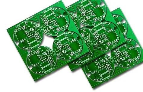
Silkscreen, often called legend printing, is a layer on a printed circuit board (PCB) that displays vital information like component labels, polarity markers, part numbers, and logos. This non-conductive ink layer is applied to the board's surface, making it easier to assemble, debug, and maintain the PCB. Without a clear silkscreen, identifying components or troubleshooting issues becomes a challenge.
The clarity of this layer depends heavily on the resolution used during printing. Resolution, measured in DPI (dots per inch), determines how sharp and detailed the silkscreen markings appear. A low DPI might result in blurry or unreadable text, while an excessively high DPI could lead to manufacturing issues or higher costs without added benefits. Understanding silkscreen DPI for PCBs is crucial for achieving the right balance between clarity and practicality.
Why Does Silkscreen Resolution Matter for PCBs?
The resolution of your silkscreen directly impacts the readability and functionality of your PCB. Here are a few reasons why PCB printing resolution is so important:
- Readability: Small text or intricate symbols on a PCB need a high enough DPI to be legible. If the resolution is too low, markings can blur or smudge, leading to assembly errors.
- Manufacturing Precision: Modern PCB manufacturing equipment has specific resolution limits. Choosing a DPI beyond these limits can cause printing errors or require specialized equipment, driving up costs.
- Cost Efficiency: Higher resolutions often mean longer printing times and more expensive processes. Striking a balance with the best silkscreen resolution saves money without sacrificing quality.
- Durability: A well-printed silkscreen using the right DPI withstands environmental factors like heat and humidity during assembly and use, ensuring long-term clarity.
By prioritizing the right silkscreen DPI for your PCB, you ensure that your design is both functional and cost-effective.
Understanding Silkscreen DPI for PCBs: What Is DPI?
DPI, or dots per inch, measures the density of dots printed in a one-inch area. In the context of PCB silkscreen, DPI indicates how detailed the printed markings will be. A higher DPI means more dots are packed into each inch, resulting in sharper and finer details. However, there's a practical limit to how high the DPI should be for PCB printing resolution.
For comparison, standard office printers often operate at 300 DPI for documents, which is sufficient for readable text on paper. However, PCBs are much smaller, and the silkscreen layer often includes tiny text or symbols (sometimes as small as 4-6 points in font size). This requires careful consideration of DPI to maintain clarity on such a small scale.
What Is the Best Silkscreen Resolution for PCBs?
Finding the best silkscreen resolution for your PCB depends on several factors, including the complexity of your design, the size of the text or symbols, and the capabilities of your manufacturing process. Here's a breakdown of common DPI ranges and their suitability:
- 150-200 DPI: This lower range is rarely used for PCBs today because it often results in blurry or unreadable markings, especially for small text or detailed symbols. It might be acceptable for very basic designs with large text, but it's generally not recommended.
- 300-400 DPI: This is the most common and widely accepted range for silkscreen DPI in PCB manufacturing. It provides a good balance between clarity and compatibility with standard printing equipment. Most manufacturers can handle this resolution without issues, and it ensures readable text down to about 6-point font size.
- 500-600 DPI: This higher resolution is ideal for intricate designs or very small markings (e.g., 4-point text). However, not all manufacturers support this level of detail, and it may increase production time and cost. Use this range only if your design demands exceptional precision.
- Above 600 DPI: Resolutions beyond 600 DPI are typically unnecessary for PCB silkscreen. They can strain manufacturing equipment, increase costs, and may not provide a noticeable improvement in clarity for most applications.
For most PCB projects, a resolution of 300-400 DPI is the sweet spot. It ensures clear, legible silkscreen markings without pushing the limits of standard manufacturing processes. Always check with your PCB manufacturer to confirm their supported DPI range before finalizing your design.
Factors Affecting Silkscreen Clarity on PCBs
While DPI is a critical factor in improving silkscreen clarity, it’s not the only consideration. Several other elements can impact the quality of your silkscreen layer. Let's explore these factors to help you achieve the best possible results:
1. Ink Type and Quality
The type of ink used for silkscreen printing plays a significant role in clarity and durability. Most PCB silkscreens use non-conductive epoxy-based inks, available in colors like white, black, or yellow. High-quality inks adhere better to the board surface and resist fading or smudging over time. Ensure your manufacturer uses reliable ink to maintain clarity at your chosen DPI.
2. Printing Method
There are different methods for applying silkscreen to PCBs, each with its own impact on resolution and clarity:
- Manual Screen Printing: This traditional method is cost-effective for simple designs but struggles with high-resolution details. It’s best suited for low-budget projects with larger text.
- Liquid Photo Imaging (LPI): This modern technique uses UV light to cure the ink, offering better precision for higher DPI settings. It’s ideal for complex designs requiring fine details.
- Direct Legend Printing: Some advanced manufacturers use inkjet-style printing for silkscreen, allowing for very high resolutions (up to 600 DPI or more) with excellent clarity.
Choose a printing method that aligns with your resolution needs and budget.
3. Font Size and Design Complexity
Even with a high DPI, tiny fonts or overly complex symbols can be hard to read if they’re not designed with manufacturing in mind. As a rule of thumb, avoid fonts smaller than 6 points at 300 DPI or 4 points at 600 DPI. Use clean, simple fonts like Arial or Helvetica for maximum legibility. Additionally, ensure sufficient spacing between characters and symbols to prevent smudging.
4. Board Surface and Color
The surface finish and color of your PCB can affect how well the silkscreen stands out. For example, white silkscreen ink on a dark green or black solder mask is highly visible, while black ink on a dark surface may be harder to read. Choose contrasting colors for better clarity, and consider the surface texture—rough surfaces may cause ink to spread slightly, reducing sharpness.
Tips for Improving Silkscreen Clarity on Your PCB
Beyond choosing the right DPI, there are several practical steps you can take to enhance the clarity of your PCB silkscreen. These tips will help ensure your markings are easy to read and durable over time:
- Optimize Your Design Files: Export your silkscreen layer at the intended DPI (e.g., 300 or 600 DPI) when preparing files for manufacturing. Avoid scaling or resizing the design after setting the resolution, as this can distort the markings.
- Use Vector Graphics: Whenever possible, design your silkscreen using vector graphics instead of raster images. Vectors maintain sharpness at any resolution, ensuring crisp text and symbols.
- Minimize Clutter: Only include essential information on the silkscreen layer. Overloading the board with unnecessary text or logos can reduce readability, especially at lower DPI settings.
- Test with Prototypes: Before mass production, order a small batch of prototypes to test silkscreen clarity. Check for readability under different lighting conditions and after assembly processes like soldering.
- Communicate with Your Manufacturer: Discuss your DPI requirements and design specifics with your PCB fabricator. They can provide guidance on the best silkscreen resolution and printing methods for their equipment.
Common Mistakes to Avoid with Silkscreen DPI for PCBs
Even experienced designers can make errors when it comes to silkscreen resolution. Here are some pitfalls to watch out for:
- Choosing an Unsupported DPI: Not all manufacturers can handle resolutions above 400 DPI. Submitting a design at 600 DPI without confirming capabilities can lead to printing errors or delays.
- Ignoring Minimum Font Sizes: Using text smaller than the recommended size for your DPI (e.g., 4-point text at 300 DPI) often results in unreadable markings.
- Overlooking Placement: Placing silkscreen text too close to pads, vias, or other board features can cause ink to bleed or become obscured during assembly. Maintain proper clearance as per industry standards (e.g., IPC guidelines suggest at least 0.2 mm spacing).
- Neglecting Color Contrast: Failing to choose a silkscreen color that contrasts with the board’s solder mask can make markings hard to read, even at high DPI.
By avoiding these mistakes, you can ensure your silkscreen layer is both clear and functional, saving time and resources during production.
How to Choose the Right DPI for Your PCB Project
Selecting the right silkscreen DPI for your PCB involves balancing design needs with manufacturing constraints. Follow this step-by-step approach to make an informed decision:
- Assess Your Design Requirements: Determine the smallest text size or symbol detail in your silkscreen layer. For text below 6 points, consider a DPI of 500-600. For larger text, 300-400 DPI is usually sufficient.
- Check Manufacturer Capabilities: Contact your PCB fabricator to confirm the DPI ranges they support. Most standard processes handle 300-400 DPI, but advanced facilities may accommodate higher resolutions.
- Consider Budget and Timeline: Higher DPI settings often increase production costs and time. If your project has tight constraints, stick to a resolution like 300 DPI unless finer detail is absolutely necessary.
- Review with a Prototype: Test your chosen DPI with a prototype run to ensure the silkscreen meets your expectations for clarity and readability.
By following these steps, you’ll land on the best silkscreen resolution for your specific PCB project, ensuring both quality and efficiency.
Conclusion: Mastering Silkscreen DPI for Better PCB Designs
Choosing the right silkscreen DPI for your PCB is a critical step in ensuring clear, readable markings that enhance the functionality and reliability of your board. By aiming for a resolution between 300 and 600 DPI—depending on your design needs and manufacturer capabilities—you can achieve the best silkscreen resolution without unnecessary costs or complications. Additionally, focusing on factors like ink quality, printing method, and design optimization will go a long way in improving silkscreen clarity.
Whether you're working on a simple prototype or a complex multilayer board, understanding PCB printing resolution and applying the tips shared in this guide will help you create professional, high-quality designs. Take the time to test your silkscreen settings, communicate with your manufacturer, and prioritize clarity in every aspect of your design process. With the right approach, your PCB silkscreen will be a valuable asset for assembly, maintenance, and beyond.
 ALLPCB


