In the world of PCB design, managing heat effectively is crucial for ensuring the performance and longevity of electronic devices. One powerful technique for achieving this is using via-in-pad thermal vias. But what exactly are via-in-pad thermal vias, and how can they help with thermal management on a PCB? Simply put, via-in-pad thermal vias are small holes placed directly under a component’s thermal pad, allowing heat to transfer efficiently from the component to a heat-dissipating layer, like a ground plane. This approach enhances heat dissipation in PCBs and boosts thermal conductivity through vias. In this blog, we’ll dive deep into the practical aspects of using via-in-pad for thermal management, covering design tips, benefits, and real-world applications for engineers looking to optimize their designs.
What Are Via-in-Pad Thermal Vias and Why Do They Matter?
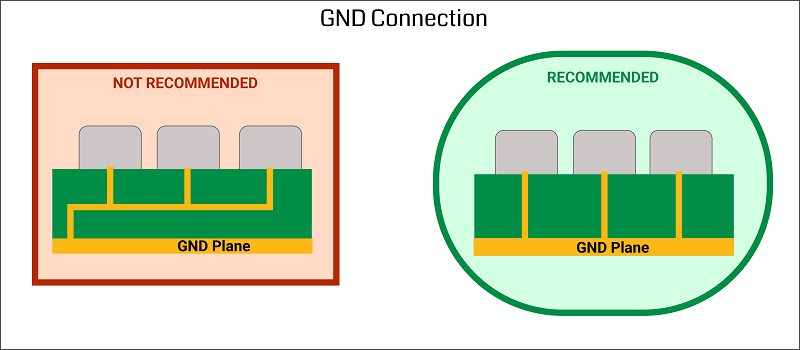
Via-in-pad refers to a design technique where vias—small conductive holes—are placed directly within the thermal pad of a surface-mounted component, such as a QFN or BGA package. Unlike traditional vias placed outside the pad, these are integrated into the pad itself, creating a direct path for heat and electrical signals. When used for thermal management, these vias act as conduits to transfer heat away from hot components to other layers of the PCB, such as copper planes or heat sinks.
The importance of via-in-pad thermal vias lies in their ability to address heat dissipation challenges in modern electronics. As devices become smaller and more powerful, components generate more heat in confined spaces. Without proper thermal management, this heat can lead to performance issues, reduced lifespan, or even component failure. By incorporating via-in-pad thermal vias, designers can achieve better thermal conductivity and maintain optimal operating temperatures, especially in high-power applications.
The Role of Thermal Vias in PCB Heat Dissipation
Thermal vias are a subset of vias specifically designed to manage heat. They create low-resistance pathways for heat to move from a component to a larger copper area or heat sink. In a typical PCB, heat generated by components like power ICs or LEDs can build up on the surface. Without a way to dissipate this heat, the component’s temperature rises, potentially exceeding safe limits (often above 85°C for many ICs).
Thermal vias help by connecting the thermal pad of a component to internal or bottom copper layers, which act as heat spreaders. For instance, a via-in-pad design might use an array of 0.3 mm diameter vias with a pitch of 1.0 mm under a component to maximize heat transfer. Studies suggest that a well-designed thermal via array can reduce thermal resistance by up to 50%, significantly lowering component temperatures.
In high-power PCBs, such as those used in automotive or industrial applications, thermal vias are often paired with large ground planes. These planes can dissipate heat over a wider area, reducing hot spots. The result is a more reliable design that can handle higher power densities without overheating.
Benefits of Using Via-in-Pad for Thermal Management
Integrating vias directly into the pad of a component offers several advantages for thermal management on a PCB. Let’s explore some key benefits:
- Enhanced Thermal Conductivity: Via-in-pad thermal vias provide a direct path for heat to flow from the component to other layers. Copper, with a thermal conductivity of about 400 W/m·K, efficiently transfers heat through these vias, reducing thermal resistance compared to designs without them.
- Space Efficiency: Modern PCB designs often face space constraints, especially in compact devices like smartphones or wearables. Via-in-pad allows for heat dissipation without requiring additional board space, as the vias are placed directly under the component.
- Improved Component Longevity: By keeping component temperatures within safe limits, via-in-pad thermal vias help prevent thermal stress, which can degrade performance or cause failure over time.
- Better Electrical Performance: In addition to thermal benefits, via-in-pad designs can reduce parasitic inductance and improve grounding for high-frequency components, enhancing overall signal integrity.
Practical Design Tips for Via-in-Pad Thermal Vias
While via-in-pad thermal vias offer significant benefits for heat dissipation in PCBs, their effectiveness depends on proper design and implementation. Here are some practical tips to ensure optimal thermal management:
1. Optimize Via Size and Spacing
The size and spacing of thermal vias play a critical role in heat transfer. Smaller vias (e.g., 0.2-0.3 mm in diameter) allow for more vias in a given area, increasing the total surface area for heat conduction. However, they must be spaced properly—typically at a pitch of 0.8-1.2 mm—to avoid manufacturing issues like solder wicking, where solder flows into the via during assembly, causing poor connections.
2. Use Copper-Filled or Plated Vias
For maximum thermal conductivity via-in-pad, consider using copper-filled or plated-through-hole vias. Copper filling enhances heat transfer by replacing air (a poor conductor) with solid copper. While this increases manufacturing costs, it can reduce thermal resistance by up to 20-30% compared to unfilled vias.
3. Connect to Large Copper Planes
Thermal vias are most effective when connected to large copper areas, such as ground or power planes, on internal or bottom layers. A copper plane with a thickness of 1 oz/ft2 (35 μm) or more can act as an effective heat spreader, dissipating heat across a wider area. Ensure these planes are uninterrupted by other traces or components to maximize their effectiveness.
4. Balance Thermal and Electrical Needs
While thermal vias are primarily for heat dissipation, they can also serve as electrical connections, especially for grounding. However, too many vias can create signal integrity issues or increase parasitic capacitance. Use simulation tools to balance thermal and electrical performance, ensuring the design meets both requirements.
5. Consider Manufacturing Constraints
Via-in-pad designs can pose challenges during PCB assembly. For instance, unfilled vias may trap air or flux, leading to voids in solder joints. To mitigate this, work with your PCB manufacturer to determine whether via tenting (covering vias with solder mask) or plugging is necessary. These processes can prevent solder wicking while maintaining thermal performance.
Real-World Applications of Via-in-Pad Thermal Vias
Via-in-pad thermal vias are widely used in industries where heat management is critical. Let’s look at a few practical examples to see how this technique is applied:
High-Power LED Lighting
In LED lighting systems, heat dissipation is a major concern due to the high temperatures generated by LED chips. A typical LED module might use a QFN package with a thermal pad connected to an array of 10-15 via-in-pad thermal vias. These vias transfer heat to a bottom copper layer, keeping the LED junction temperature below 100°C, even under continuous operation at 5W or more.
Automotive Electronics
Automotive control units often include power management ICs that generate significant heat. Via-in-pad thermal vias under these components connect to thick copper planes, ensuring heat is dissipated effectively. This is critical in harsh environments where ambient temperatures can exceed 60°C, and component reliability is non-negotiable.
Consumer Electronics
In compact devices like smartphones, space is limited, and components like processors or RF modules generate substantial heat. Via-in-pad designs allow for efficient thermal management without increasing the PCB footprint. For example, a processor with a thermal pad might use 20 microvias (0.1 mm diameter) to channel heat to an internal ground plane, maintaining temperatures within safe limits during peak usage.
Challenges and Limitations of Via-in-Pad Thermal Vias
While via-in-pad thermal vias are highly effective for thermal management on a PCB, they come with some challenges that designers must address:
- Manufacturing Complexity: Placing vias directly under a pad can complicate the assembly process. Issues like solder wicking or voiding can occur if vias are not properly filled or tented, potentially leading to unreliable connections.
- Cost Considerations: Copper-filled vias or advanced manufacturing techniques to prevent assembly issues can increase production costs. Designers must weigh these costs against the thermal benefits.
- Design Trade-Offs: Adding numerous thermal vias can impact the PCB’s mechanical strength or interfere with routing on other layers. Careful planning is needed to avoid compromising the overall design.
Despite these challenges, the benefits of via-in-pad thermal vias often outweigh the drawbacks, especially in high-performance applications where heat dissipation is a priority.
Advanced Techniques for Enhancing Thermal Conductivity Via-in-Pad
For designs requiring even greater heat dissipation, consider these advanced techniques alongside via-in-pad thermal vias:
- Thermal Pads with Exposed Copper: Expose a large copper area on the bottom layer connected to thermal vias. This can be paired with a heat sink or thermal interface material to further dissipate heat.
- Multi-Layer Heat Spreading: Use multiple internal copper layers connected by thermal vias to distribute heat more evenly across the PCB. For example, a 4-layer board might dedicate two layers to heat spreading, reducing thermal resistance by up to 40%.
- Active Cooling Integration: In extreme cases, thermal vias can work in conjunction with active cooling solutions like fans or liquid cooling systems. Vias transfer heat to a designated layer, where it is then removed by the cooling system.
Conclusion: Mastering Thermal Management with Via-in-Pad
Effective thermal management is a cornerstone of reliable PCB design, and via-in-pad thermal vias offer a practical, space-efficient solution for heat dissipation in PCBs. By placing vias directly under component pads, designers can achieve superior thermal conductivity, reduce hot spots, and extend the lifespan of critical components. Whether you’re working on high-power LEDs, automotive electronics, or compact consumer devices, incorporating via-in-pad thermal vias into your design can make a significant difference.
Remember to optimize via size and spacing, connect to large copper planes, and account for manufacturing constraints to get the best results. While challenges like cost and complexity exist, the benefits of improved thermal management often justify the effort. With the right approach, via-in-pad thermal vias can help you create robust, high-performance PCB designs that stand up to the demands of modern electronics.
By leveraging these strategies, you can ensure your designs not only meet thermal requirements but also deliver long-term reliability and efficiency. Start integrating via-in-pad thermal vias into your next project and experience the difference in thermal management firsthand.
 ALLPCB


