 ALLPCB


Introduction
Printed Circuit Board (PCB) design is at the heart of modern electronics, enabling everything from smartphones and IoT devices to advanced robotics and AI-driven systems. As electronics evolve in complexity and performance, PCB design becomes more critical, impacting product reliability, efficiency, and innovation. In 2025, PCB design is not just about connecting components—it’s about managing high-speed signals, power efficiency, thermal performance, and manufacturability. Applications span across consumer electronics, automotive, aerospace, medical devices, and industrial automation, making PCB design a cornerstone of the electronics industry.
PCB Design Basics
PCBs are built from layers of conductive copper traces, insulating substrates, vias, and pads. At the foundation, a PCB consists of:
- Substrate (FR4, polyimide, etc.): Provides structural stability and thermal support. FR4 is common, while polyimide is used for high-temperature applications.
- Copper Layers: Conductive traces carry electrical signals. PCBs can be single-layer, double-layer, or multilayer, with inner layers often used for power distribution or signal routing.
- Solder Mask: Protects copper traces from shorts and oxidation, ensuring solder adheres only to exposed pads.
- Silkscreen: Prints reference markings, component IDs, and symbols for assembly guidance.
- Vias and Pads: Vias connect traces across layers; pads are exposed copper areas for soldering components.
The PCB design process generally includes:
- Schematic Capture: Convert the circuit into a schematic diagram defining components and connections.
- Component Placement: Position parts considering functionality, manufacturability, and thermal management.
- Routing: Connect components with traces, maintaining signal integrity and proper spacing.
- Design Rule Check (DRC): Verify trace widths, spacing, and other parameters to ensure manufacturability.
- Gerber File Generation: Produce standardized files for fabrication and assembly, describing each layer and drill locations.
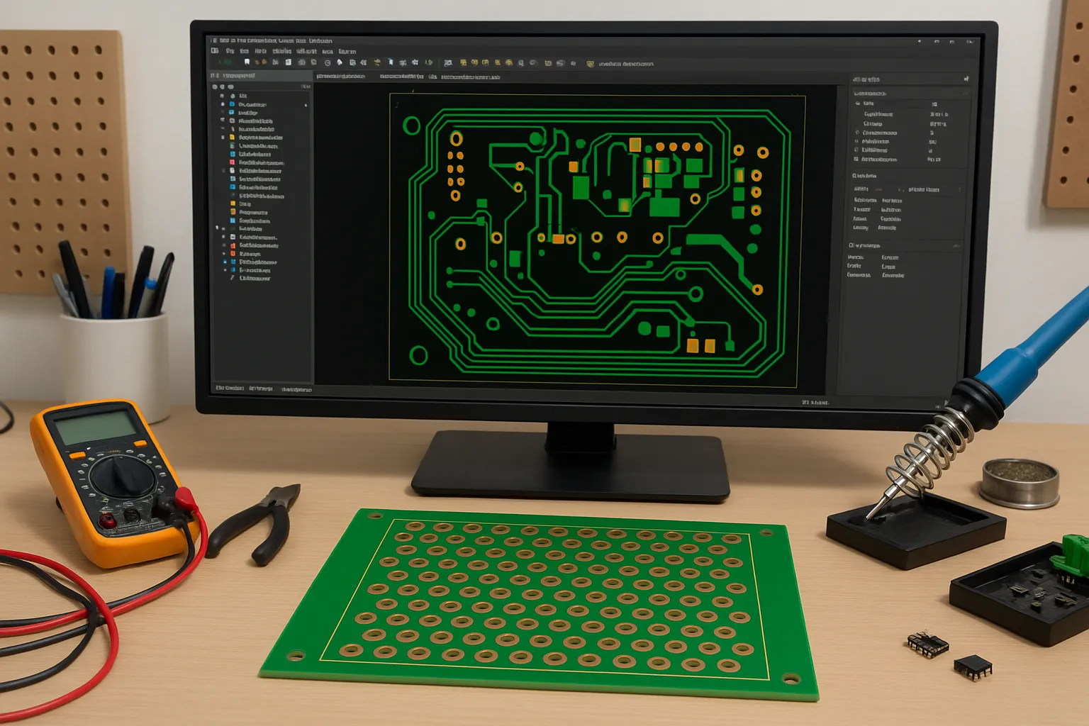
Design Tools & Software
Choosing the right PCB design softwares is essential for engineers in 2025, as tools directly impact workflow efficiency, signal accuracy, and manufacturability. Among the most widely used platforms are Altium Designer, Cadence Allegro, OrCAD, KiCad, Autodesk Eagle, and Siemens EDA solutions. Each software serves different needs: Altium is strong in advanced routing and 3D visualization, Allegro excels in high-speed and enterprise-level projects, KiCad provides powerful open-source flexibility, and Eagle integrates seamlessly with mechanical CAD for IoT and prototyping.
As PCB design evolves, software tools are moving toward greater intelligence and collaboration. AI-assisted design now helps automate routing and detect errors, while cloud-native platforms enable real-time teamwork across global design teams. Features such as 3D visualization, simulation for signal integrity and thermal performance, and built-in DFM checks are becoming standard. Staying updated with these advances ensures designers can handle the growing complexity of high-speed circuits, flexible PCBs, and next-generation IoT and AI hardware.
Design Considerations
Designing a PCB requires balancing multiple engineering domains:
Electrical Considerations
Signal performance is critical. Parameters such as PCB copper thickness influence current capacity and thermal performance. Controlled impedance routing ensures stability in high-speed circuits. Engineers often apply impedance control techniques to maintain signal quality.
Mechanical Considerations
Form factor and durability matter. Designers must consider board shape, thickness, and mounting holes for structural stability. Flexible PCBs are often used in compact devices like wearables.
Thermal Considerations
Managing heat is essential to reliability. Engineers employ heat sinks, copper pours, and thermal vias to distribute and dissipate heat efficiently.
Manufacturing Feasibility
Manufacturability is considered throughout the process. Ensuring DFM practices early reduces costly redesigns and production delays.
Advanced PCB Design
As electronics push boundaries, advanced PCB design techniques are necessary:
- High-speed design – Handling GHz-level signals requires precise routing, controlled impedance, and careful via design to minimize reflections and losses. Techniques such as differential pair routing, ground planes, and signal integrity simulations are critical in supporting PCIe 6.0/7.0, DDR5/DDR6 memory, and other high-speed interfaces.
- Multilayer PCBs – With component density increasing, multilayer boards provide better routing flexibility and improved electromagnetic shielding. Optimized stack-up design reduces crosstalk and enhances power integrity, making them indispensable in servers, 5G base stations, and aerospace applications.
- RF & microwave design – Wireless technologies like 5G, Wi-Fi 7, and automotive radar demand PCBs designed with strict impedance control and low-loss materials. Special substrates such as Rogers or PTFE are used to maintain performance at high frequencies.
- Flexible & rigid-flex PCBs – These are increasingly vital in compact, lightweight, and durable designs such as wearables, medical implants, drones, and satellites. Rigid-flex technology allows seamless integration between rigid sections for stability and flexible sections for mobility.
- AI-driven design – Modern EDA tools now integrate AI to assist with auto-routing, component placement, and error detection. AI can predict signal integrity issues, optimize thermal management, and even suggest cost-effective layouts, reducing design cycles and improving first-pass success rates.

Common Challenges & Solutions
Even experienced designers face issues:
- EMI (Electromagnetic Interference) – High-speed signals, poor grounding, or improper layer stack-ups can cause radiation and coupling problems. Solutions include maintaining continuous ground planes, optimizing trace layout, and applying effective shielding techniques. For more details, see practices related to EMI control in PCB design.
- Signal Integrity Issues – At GHz-level speeds, reflections, crosstalk, and delay skew can severely degrade signal quality. Designers address these with impedance matching, controlled trace lengths, and simulation-based validation. Learn more about managing signal integrity issues in high-speed PCB design.
- Thermal Management – Heat buildup can shorten component lifespan and reduce system reliability. Thermal vias, copper pours, and heatsinks are commonly used to improve dissipation. Advanced strategies, such as thermal vias, are essential in high-power applications.
- Impedance Control – Incorrect impedance can cause reflections and distort high-speed signals. Proper stack-up design, trace width calculation, and material selection are critical. Detailed approaches to impedance control are necessary in RF and high-speed PCBs.
- Manufacturability Challenges – Designs that ignore fabrication limits may lead to defects or higher production costs. Applying DFM principles ensures that layouts meet manufacturing tolerances while optimizing yield. A dedicated discussion on DFM highlights best practices for aligning design with production capabilities.
By integrating simulation tools and best practices, these challenges can be resolved efficiently.
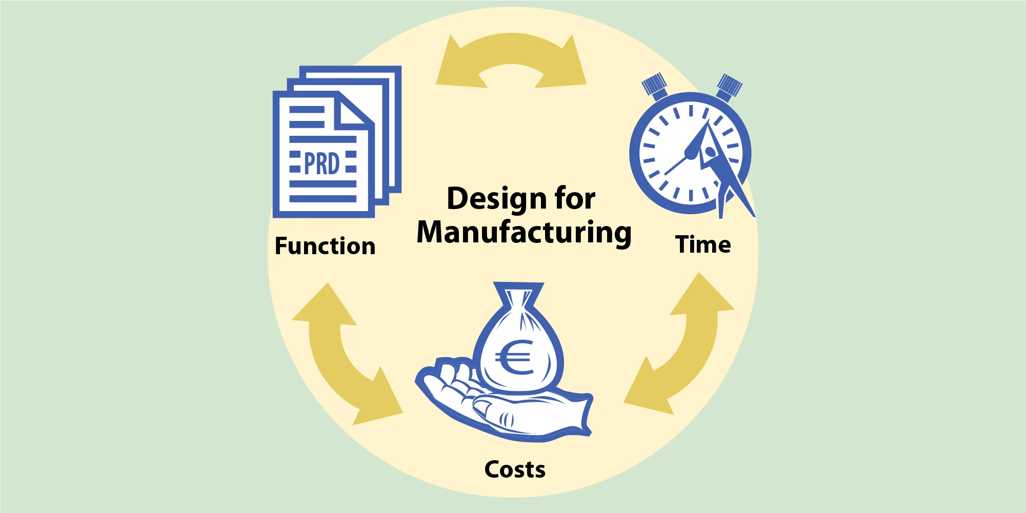
PCB Manufacturing & Assembly
Designing a PCB is only half the journey — ensuring smooth manufacturing and assembly is equally critical. A design that performs well in simulation may still fail if it cannot be fabricated or assembled efficiently. This is why close collaboration between designers and manufacturers is essential.
One of the most important principles is DFM (Design for Manufacturing), which ensures that layouts comply with fabrication tolerances such as minimum trace widths, via sizes, and copper clearances. Applying DFM guidelines early helps reduce defects, improve yields, and lower overall costs. Similarly, DFT (Design for Testability) must be considered to provide test points and access for debugging during assembly and quality control.
Modern PCB manufacturing also relies heavily on precision processes such as automated solder paste printing, pick-and-place assembly, and reflow soldering. For advanced boards, techniques like selective soldering, X-ray inspection, and AOI (Automated Optical Inspection) ensure quality and reliability. In high-power or high-frequency designs, features such as controlled copper thickness, thermal vias, and surface finishes (ENIG, HASL, OSP) must be optimized to balance electrical and mechanical performance.
In 2025, the integration of smart factories and AI-driven quality assurance is transforming PCB production. Intelligent inspection systems detect defects in real time, while digital twins allow manufacturers to simulate assembly workflows before production. By aligning PCB design closely with fabrication and assembly requirements, engineers can ensure a seamless transition from concept to mass production, reducing both lead time and risk.
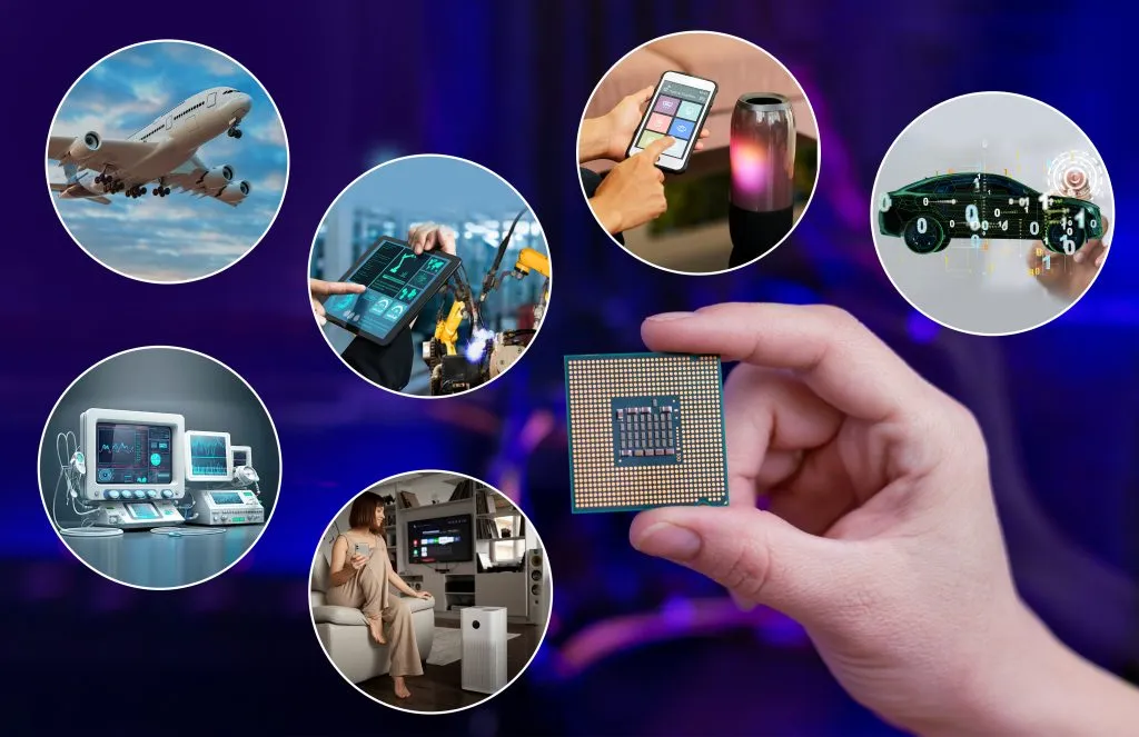
Applications of PCB Design
PCB design supports innovation across industries:
-
IoT – Compact, low-power PCBs drive wearables, smart sensors, and connected devices. Learn more about IoT PCB design.
-
Robotics – From motor controllers to AI processors, PCBs power robotics systems. See practical examples in robotics PCB design.
-
AI hardware – AI accelerators demand advanced PCBs for thermal control and high-speed data. Explore AI-driven PCB design.
-
Consumer electronics – Smartphones, laptops, and wearables rely on optimized PCB design for performance and miniaturization.
-
Automotive & aerospace – Safety-critical and ruggedized PCBs handle extreme conditions.
Conclusion
PCB design is the foundation of electronics innovation in 2025. Mastery of fundamentals such as copper thickness, impedance control, thermal vias, EMI, and DFM is essential for building reliable systems. With AI and IoT shaping the future, PCB designers must stay agile, combining proven practices with emerging technologies to deliver the next generation of electronic devices.


