 ALLPCB


The Internet of Things (IoT) is transforming industries, from smart homes to industrial automation, by connecting devices that collect and share data seamlessly. At the heart of every IoT device lies a printed circuit board (PCB), meticulously designed to balance power efficiency, compact size, and robust connectivity. For engineers, achieving this balance is a complex challenge that demands precision and innovation. In this blog, we explore the key considerations and strategies for designing IoT PCBs that meet the stringent demands of modern applications, offering practical insights to help you succeed in your next project.
Whether you're developing a wearable health monitor or an industrial sensor, understanding how to optimize power, size, and connectivity is critical. Let's dive into the core principles and techniques that drive effective IoT PCB design.
Understanding IoT PCB Design Challenges
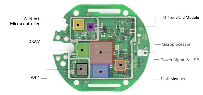
IoT devices are defined by their ability to sense, process, and communicate data, often in compact form factors with limited power sources. This creates unique challenges for PCB designers. Devices must operate efficiently on battery power, fit into small enclosures, and maintain reliable wireless connections in diverse environments. For example, a smart thermostat might need to fit within a 100 mm x 100 mm enclosure while supporting Wi-Fi connectivity and running on a single CR2032 battery for over a year.
The primary challenges include:
- Power Efficiency: IoT devices often rely on batteries or energy harvesting, requiring designs that minimize power consumption without sacrificing performance.
- Miniaturization: Compact layouts are essential for wearables, sensors, and other space-constrained applications.
- Connectivity: Robust wireless communication, such as Bluetooth, Wi-Fi, or Zigbee, must be maintained despite potential interference and signal degradation.
Addressing these challenges requires a strategic approach to component selection, layout design, and signal integrity management.
Optimizing Power Efficiency in IoT PCBs
Power efficiency is a cornerstone of IoT PCB design, as many devices operate on limited energy sources. Achieving long battery life—often exceeding 12 months—requires careful component selection and power management strategies.
Selecting Low-Power Components
Choosing components with low power consumption is critical. For example, microcontrollers (MCUs) like the STM32WBA52 from STMicroelectronics, which supports Bluetooth LE 5.3 with ultra-low-power modes, can reduce power draw to as low as 1 µA in standby mode. Similarly, sensors such as temperature or pressure sensors should have low quiescent currents, ideally below 10 µA, to minimize energy use during idle periods.
Implementing Power Management Techniques
Effective power management involves techniques like clock gating and sleep modes. Clock gating disables clocks to unused components, reducing dynamic power consumption by up to 30%. Deep sleep modes allow MCUs and wireless modules to enter low-power states, consuming less than 5 µW when idle. For instance, in a smart meter, the MCU can wake up every 10 seconds to transmit data, spending the majority of its time in sleep mode to extend battery life.
Another strategy is power budgeting, where each circuit block is allocated a specific power limit. For example, a wearable device might allocate 50 mW to the MCU, 20 mW to the sensor, and 30 mW to the wireless module, ensuring the total power draw stays within the battery's capacity.
Energy Harvesting
In remote or off-grid applications, energy harvesting—using solar, kinetic, or thermal energy—can supplement or replace batteries. A PCB designed for energy harvesting might include a power management IC like the Texas Instruments BQ25504, which efficiently manages energy from a solar cell with a conversion efficiency of up to 90%.
Achieving Compact PCB Layouts
Miniaturization is a hallmark of IoT devices, enabling applications like smartwatches and medical implants. However, packing more functionality into smaller spaces increases design complexity.
High-Density Interconnect (HDI) Technology
HDI PCBs use microvias (diameters as small as 50 µm) and fine-line traces (widths below 100 µm) to increase component density. This allows designers to integrate more components, such as sensors and communication modules, within a compact footprint. For example, an HDI PCB for a fitness tracker might use a 6-layer stack-up to route signals efficiently in a 20 mm x 30 mm board.
Flexible and Rigid-Flex PCBs
Flexible and rigid-flex PCBs are ideal for devices with non-standard shapes or tight spaces. Flexible PCBs, made from polyimide, can bend or fold, reducing the need for connectors and saving up to 50% in volume compared to rigid boards. A rigid-flex PCB in a smartwatch might combine a rigid section for the MCU and a flexible section for the display, fitting into a curved enclosure.
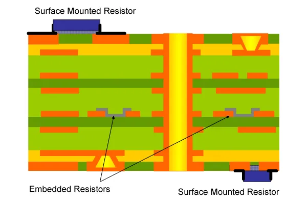
Embedded Components
Embedding passive and active components within the PCB substrate reduces surface area requirements. For instance, embedding a 10 µF capacitor within the board layers can save 2 mm² of surface space, improving signal integrity by shortening trace lengths. This technique is particularly useful in medical devices where size is critical.
Ensuring Robust Connectivity
Reliable wireless connectivity is the backbone of IoT devices, enabling seamless data exchange across protocols like Bluetooth, Wi-Fi, Zigbee, or 5G. However, maintaining signal integrity in high-density layouts and crowded RF environments is a significant challenge.
Antenna Design and Placement
Antenna integration is critical for wireless performance. Printed antennas, such as planar inverted-F antennas (PIFAs), can be embedded within the PCB to save space. For a 2.4 GHz Bluetooth module, the antenna trace length should be approximately 31 mm to match the quarter-wavelength requirement. Placement is equally important—antennas should be positioned away from metal components and ground planes to avoid interference, ideally with a clearance of at least 10 mm.
Signal Integrity and EMI Mitigation
High-frequency signals in IoT devices are susceptible to degradation due to crosstalk and electromagnetic interference (EMI). To maintain signal integrity, designers should use controlled impedance traces, typically set at 50 ohms for RF signals, and incorporate ground planes to reduce noise. Shielding techniques, such as adding a copper pour around sensitive components, can reduce EMI by up to 20 dB. For example, in a smart home sensor, separating analog and digital signals on different layers can prevent crosstalk, ensuring reliable data transmission.
Leveraging ALLPCB’s Expertise for IoT Success
At ALLPCB, we understand the complexities of IoT PCB design and offer tailored solutions to help engineers achieve optimal results. Our quick-turn prototyping services deliver high-quality PCBs in as little as 24 hours, enabling rapid iteration and testing. With advanced manufacturing capabilities, including HDI and flexible PCB production, we ensure your designs meet the highest standards for power efficiency, size, and connectivity. Our global logistics network guarantees fast delivery, and our expert team provides design-for-manufacturability (DFM) feedback to optimize your layouts. Whether you're developing a prototype or scaling to production, ALLPCB is your trusted partner for bringing innovative IoT devices to market efficiently.
Conclusion
Designing PCBs for IoT devices requires a delicate balance of power efficiency, compact size, and robust connectivity. By leveraging low-power components, advanced layout techniques like HDI and flexible PCBs, and robust antenna and signal integrity strategies, engineers can create devices that meet the demands of modern applications. With careful planning and the right manufacturing partner, your IoT designs can achieve exceptional performance and reliability.
Ready to bring your IoT vision to life? Partner with ALLPCB to transform your concepts into reality with precision and speed.


