Designing high-power printed circuit boards (PCBs) comes with unique challenges, especially when it comes to grounding. Proper PCB grounding techniques are vital for ensuring a reliable and safe electronic design. If you're working on high-power boards, effective grounding minimizes electromagnetic interference (EMI), reduces noise, and protects components from damage due to high currents and voltages. In this comprehensive guide, we'll dive deep into the best grounding strategies for high-power PCBs, offering practical tips and detailed insights to help you achieve optimal performance and safety.
Why Grounding Matters for High-Power PCBs
Grounding serves as the backbone of any electronic design, providing a common reference point for all signals and power in a circuit. For high-power PCBs, where currents can exceed 10A and voltages may reach hundreds of volts, grounding is even more critical. Poor grounding can lead to issues like signal distortion, excessive heat, and even catastrophic failures such as short circuits or component burnout. By implementing robust PCB grounding techniques, you ensure stability, safety, and efficiency in your designs.
Key Challenges in Grounding High-Power Boards
High-power PCBs face specific challenges that make grounding more complex compared to low-power designs. These include:
- High Currents: Large currents can cause significant voltage drops across ground paths if not managed properly, leading to noise and instability.
- Heat Dissipation: High power generates heat, which can affect ground plane performance if thermal management isn’t integrated into the design.
- EMI and Noise: High-frequency switching in power circuits often produces EMI, which can interfere with nearby components or signals.
- Dense Layouts: High-power boards often have tight layouts, making it harder to allocate space for effective grounding.
Understanding these challenges is the first step toward applying the right PCB grounding techniques to overcome them.
Essential PCB Grounding Techniques for High-Power Boards
Let’s explore some proven grounding strategies tailored for high-power PCB designs. These techniques focus on maintaining signal integrity, reducing EMI, and ensuring safety.
1. Use Dedicated Ground Planes
A dedicated ground plane is a large, continuous layer of copper on your PCB that acts as a low-impedance path for return currents. For high-power boards, a ground plane is non-negotiable. It minimizes ground loops and provides a stable reference point for all components. Studies suggest that a well-designed ground plane can reduce EMI by up to 20 dB in high-frequency circuits.
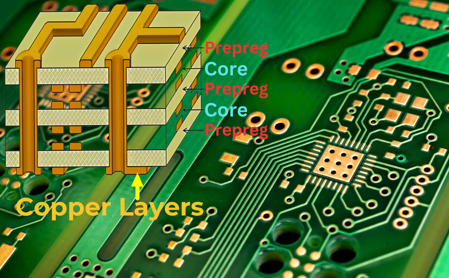
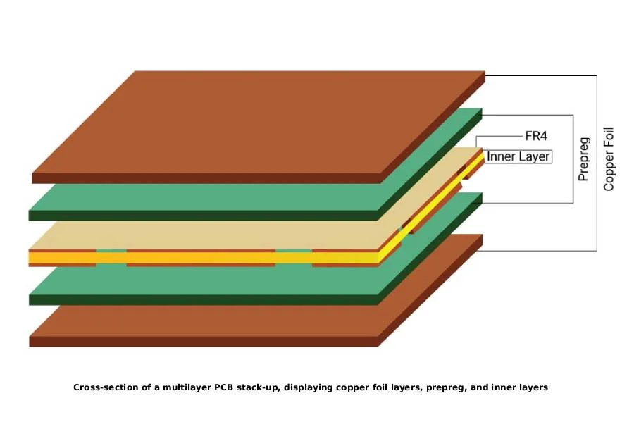
Implementation Tip: Place the ground plane directly below the power layer in a multilayer PCB stack-up. Ensure it covers as much area as possible, avoiding splits or cuts that could disrupt current flow. For boards handling currents above 5A, consider using multiple ground planes to further reduce impedance.
2. Implement Ground Vias Strategically
Ground vias connect different layers of a PCB to the ground plane, ensuring a low-resistance path for return currents. In high-power designs, place ground vias near high-current components like power transistors or capacitors to minimize voltage drops. A typical design might use vias with a diameter of 0.3mm to 0.5mm, spaced every 10mm around critical areas, to maintain low impedance.
Implementation Tip: Avoid placing vias too close to each other, as this can weaken the board structure. Instead, distribute them evenly to balance current flow and structural integrity.
3. Separate Analog and Digital Grounds
In high-power boards that include both analog and digital circuits, mixing their ground paths can introduce noise and interference. Analog signals are sensitive to the high-frequency noise often generated by digital components. To prevent this, use separate ground planes for analog and digital sections, connecting them at a single point near the power supply to avoid ground loops.
Implementation Tip: For boards with mixed signals, route analog components on one side of the PCB and digital components on the other, with a clear boundary between their respective ground planes.
4. Minimize Ground Loops
Ground loops occur when return currents take multiple paths back to the source, creating unwanted noise and EMI. In high-power designs, ground loops can be particularly problematic due to the large currents involved. To avoid this, ensure that all components connect to the ground plane through the shortest possible path.
Implementation Tip: Use a star grounding topology for critical components, where each component connects directly to a central ground point rather than forming a loop. This can reduce noise by up to 30% in high-current applications.
5. Optimize for High-Current Paths
High-power boards often deal with currents exceeding 10A, which can cause significant voltage drops if ground paths are too narrow or long. To handle this, use wider traces or even copper pours for ground connections in high-current areas. A general rule of thumb is to design ground traces to handle at least 1.5 times the expected current to account for transients.
Implementation Tip: Calculate trace width using a PCB design tool or standard charts to ensure it can carry the current without overheating. For example, a 1oz copper trace carrying 10A may need to be at least 200 mils wide at room temperature.
6. Incorporate Galvanic Isolation
For high-power boards operating at high voltages (above 100V), galvanic isolation is a safety must. It prevents dangerous currents from flowing between different sections of the board, protecting both the circuit and the user. Isolation can be achieved using optocouplers or transformers, with ground planes separated between isolated sections.
Implementation Tip: Ensure that isolated ground planes do not overlap, and maintain a clearance of at least 8mm between high-voltage and low-voltage sections to prevent arcing.
Advanced Grounding Strategies for High-Power Designs
Beyond the basics, there are advanced PCB grounding techniques that can further enhance the reliability of high-power boards, especially in complex or high-frequency applications.
7. Use Split Ground Planes for Mixed-Signal Designs
In boards with both high-power and sensitive low-power signals, a split ground plane can be effective. This involves dividing the ground plane into distinct sections for different circuit types (e.g., power, control, and sensing) while connecting them at a single point to avoid loops. This method reduces crosstalk and noise coupling between sections.
Implementation Tip: When splitting ground planes, route signals over their respective ground sections to maintain return path continuity. Avoid crossing signals over splits, as this can increase EMI.
8. Integrate Decoupling Capacitors Near Power Pins
Decoupling capacitors help stabilize voltage levels by filtering out noise near power pins of ICs and other components. In high-power designs, place these capacitors as close as possible to the pins, with a direct connection to the ground plane. Use a combination of capacitor values (e.g., 0.1μF and 10μF) to cover a wide range of frequencies.
Implementation Tip: Ensure the ground connection for each capacitor is short and direct, ideally less than 5mm, to minimize inductance.
Suggested Image Placement: Include a schematic here showing decoupling capacitors near IC power pins connected to a ground plane. ALT Text: "Decoupling capacitors near IC pins for PCB grounding."
9. Consider Chassis Grounding for Safety
In high-power applications, connecting the PCB ground to the chassis ground can provide an additional layer of safety. This ensures that any fault currents are safely directed away from sensitive components and users. Chassis grounding is especially important in industrial or automotive designs where high voltages are common.
Implementation Tip: Use a dedicated mounting hole or connector to link the PCB ground to the chassis, ensuring a low-resistance path with a current rating that matches or exceeds the system’s maximum fault current.
Common Grounding Mistakes to Avoid in High-Power PCB Design
Even with the best intentions, certain grounding mistakes can compromise the performance and safety of high-power boards. Here are a few pitfalls to watch out for:
- Insufficient Ground Plane Coverage: A ground plane with gaps or cuts can disrupt return currents, increasing noise and EMI. Always aim for a continuous plane wherever possible.
- Overloading Ground Traces: Undersized ground traces can overheat under high current, leading to board failure. Double-check current ratings during design.
- Ignoring Thermal Effects: High currents generate heat, which can affect ground plane performance. Integrate thermal vias or heat sinks to manage temperature.
- Mixing Ground Types Without Isolation: Combining digital, analog, and power grounds without proper separation can introduce noise into sensitive circuits.
Tools and Resources for Effective PCB Grounding
Designing grounding for high-power PCBs is easier with the right tools. Many PCB design software platforms offer simulation features to analyze ground plane performance, current distribution, and EMI. Use these tools to test your grounding strategy before manufacturing. Additionally, refer to industry standards like IPC-2221 for guidelines on trace widths, clearances, and grounding practices.
Conclusion: Building Reliable High-Power PCBs with Proper Grounding
Effective PCB grounding techniques are the foundation of a reliable and safe electronic design, especially for high-power boards. By using dedicated ground planes, strategic vias, separate ground sections, and other methods discussed in this guide, you can minimize noise, reduce EMI, and ensure the longevity of your design. High-power applications demand careful planning and attention to detail, but with the right grounding strategies, you can achieve outstanding performance and safety.
Start implementing these PCB grounding techniques in your next high-power project to see the difference they make. A well-grounded design not only performs better but also protects your components and users from potential hazards. With the tips and insights shared here, you’re well-equipped to tackle the challenges of high-power PCB design with confidence.
 ALLPCB


