 ALLPCB


In the fast-evolving world of electronics, printed circuit boards (PCBs) are the backbone of nearly every device we rely on. As these boards grow smaller and more intricate, ensuring their quality becomes a daunting challenge. Hidden defects—like solder voids or misaligned components—can lead to failures that cost time, money, and even safety in critical applications. That's where X-ray inspection steps in. This powerful, non-destructive technology peers beneath the surface of PCBs to reveal issues invisible to the naked eye or traditional methods. For engineers, understanding X-ray inspection is key to producing reliable, high-performance electronics.
In this blog, we'll dive into how X-ray inspection works, the defects it uncovers, and why it's a game-changer in PCB assembly. From its unique advantages to real-world applications, we'll provide practical insights to help you ensure your PCBs meet the highest standards. Let's explore how this technology keeps modern electronics dependable and defect-free.
What is X-Ray Inspection in PCB Assembly?
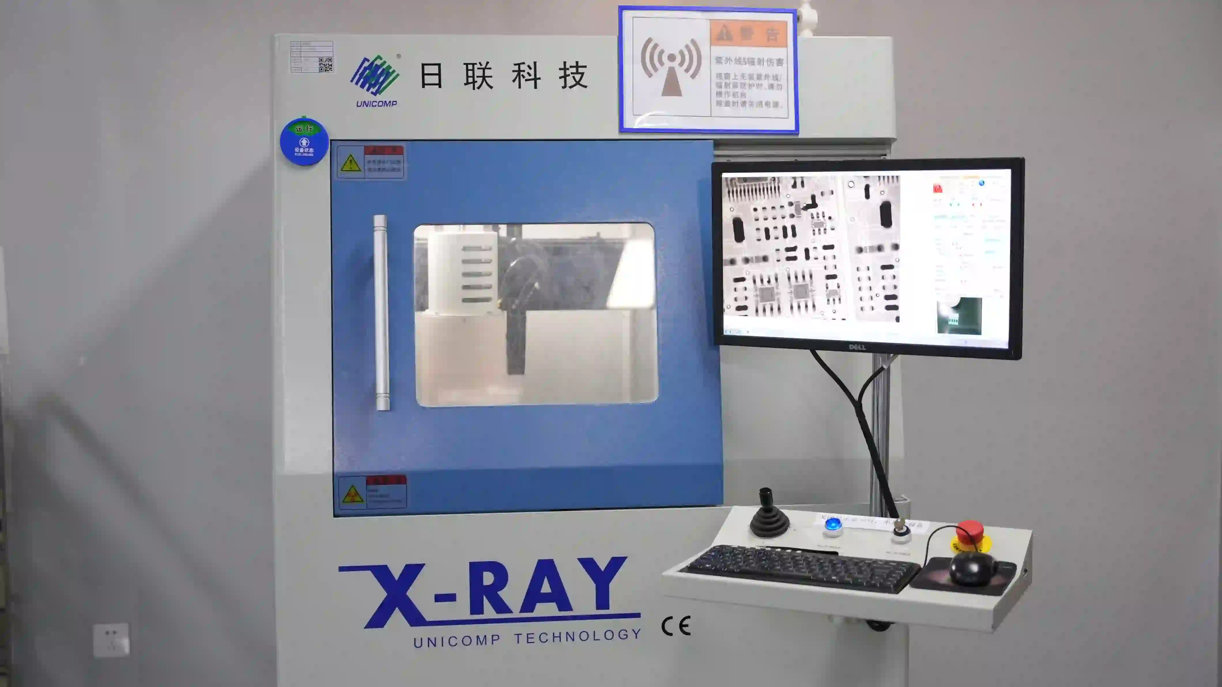
X-ray inspection, often called automated X-ray inspection (AXI), is a non-destructive testing method that uses X-ray radiation to examine the internal features of a PCB. Unlike surface-level checks, it reveals hidden solder joints, internal cracks, and other defects in complex or multilayer boards. This makes it indispensable as PCB designs pack more components—like ball grid arrays (BGAs)—into tighter spaces, where traditional inspection falls short.
For engineers, X-ray inspection is a lifeline. It ensures that every connection, even those buried under layers or components, is sound. By catching defects early, it prevents costly rework and boosts reliability in everything from smartphones to aerospace systems.
How X-Ray Inspection Works
X-ray inspection relies on a straightforward yet sophisticated setup: an X-ray source, a detector, and a movable platform holding the PCB. Here's how it operates:
1. X-Ray Emission: The source fires X-rays that pass through the PCB. Materials absorb these rays differently based on their density and atomic weight—heavier elements like solder block more X-rays, while lighter ones like the substrate let more through.
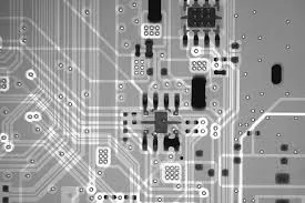
2. Image Creation: A detector on the opposite side captures the X-rays that make it through, turning them into a digital image. Dense areas (like solder) show up darker, while less dense areas (like the board) appear lighter.
3. Defect Detection: Software analyzes the image, flagging irregularities like voids or bridges by comparing it to a perfect model or using algorithms to spot anomalies.
This process is fast and precise, often taking just seconds per board. Advanced systems can even rotate the PCB or use computed tomography (CT) for 3D views, offering engineers a complete picture of internal quality.
Suggested Reading:PCB X-ray Inspection for Beginners: A Step-by-Step Guide
Types of Defects Detected by X-Ray Inspection
X-ray inspection shines at finding defects that other methods miss. Here are the key issues it uncovers:
1. Solder Voids
Solder voids are tiny gas bubbles trapped in a solder joint, often from flux outgassing during reflow. They weaken the joint's strength and conductivity—studies show voids over 25% of a joint's area can cut reliability by up to 50%. X-ray spots these as lighter patches in the darker solder mass.
2. Solder Bridges
When solder accidentally connects adjacent pins or pads, you get a bridge—a recipe for short circuits. In dense boards with pitches as tight as 0.4 mm, bridges are a growing risk. X-ray reveals these unwanted links clearly, even under components.
3. Insufficient or Excess Solder
Too little solder risks weak joints; too much can spill over and cause shorts. X-ray images show solder volume, helping engineers ensure joints meet specs—typically 50-75% fill for BGAs, per IPC standards.
4. Misaligned Components
Misplaced parts, especially BGAs or quad flat no-leads (QFNs), can disrupt connections. X-ray aligns the actual position against the design, catching shifts as small as 0.1 mm that could kill a board's performance.
5. Internal Cracks and Delamination
Cracks in vias or delamination between layers threaten a PCB's structure and signals. X-ray, especially with CT, exposes these flaws, which can reduce a board's lifespan by 30% if undetected.
These capabilities make X-ray a must-have for high-stakes projects where failure isn't an option.
Benefits of X-Ray Inspection in PCB Assembly
X-ray inspection isn't just a tool—it's a competitive edge. Here's why engineers swear by it:
1. Non-Destructive Testing
Unlike cutting a board apart, X-ray checks quality without harm. This saves valuable prototypes and keeps production rolling, cutting waste by up to 15% in some workflows.
2. Visibility of Hidden Features
With multilayer PCBs now common—over 60% of boards in consumer electronics have 4+ layers—X-ray's ability to see inside is unmatched. It inspects joints under BGAs or QFNs that optical methods can't touch.
3. Better Quality Control
Catching defects early slashes rework costs by 20-30%, per industry estimates. Real-time X-ray feedback lets you tweak soldering or placement on the fly, keeping quality tight.
4. Reliability for Critical Use
In fields like medical or automotive, where failure rates must stay below 0.1%, X-ray ensures every board holds up. It's why 90% of aerospace PCB makers use it for final checks.
These perks translate to fewer headaches and higher trust in your end product.
Suggested Reading:Unveiling Hidden Defects: A Deep Dive into PCB Assembly X-Ray Inspection
Comparison with Other Inspection Methods
X-ray isn't the only game in town—Automated Optical Inspection (AOI) is a popular alternative. Here's how they stack up:
X-Ray Inspection vs. AOI
- AOI: Uses cameras and light to scan a PCB's surface. The AOI inspection is quick (under 10 seconds per board) and great for spotting missing parts or surface bridges. But it's blind to what's beneath—hidden joints are its kryptonite.
- X-Ray: Slower (30-60 seconds per board) and pricier, but it sees everything. It's the go-to for internal defects in complex assemblies, catching what AOI misses 80% of the time in multilayer boards.
Together, they're a one-two punch: AOI for speed, X-ray for depth.
Applications of X-Ray Inspection in PCB Assembly
X-ray's versatility makes it a staple across the assembly process:
1. Post-Soldering Checks
After reflow, X-ray verifies solder joints—crucial for BGAs, where 70% of defects like voids occur. It ensures every connection is solid before moving forward.
2. Component Screening
Incoming ICs can hide cracks or fakes. X-ray vets them, catching 95% of internal flaws that could derail assembly, per quality audits.
3. Final QA
Before shipping, X-ray confirms the whole board's integrity. For high-reliability PCBs, it's the last line of defense, ensuring zero defects in 99.9% of cases.
4. Failure Analysis
When a board fails, X-ray pinpoints why—whether it's a cracked via or a bad joint. This cuts diagnosis time by half, speeding up fixes.
From start to finish, X-ray keeps quality on lock.
How ALLPCB Supports Engineers with Advanced Inspection
At ALLPCB, we know engineers need PCBs they can count on. Our cutting-edge X-ray inspection catches hidden defects, ensuring your boards perform flawlessly—whether it's a quick prototype or a full production run. With global logistics and advanced manufacturing, we deliver fast, reliable solutions tailored to your needs. Our expertise in high-density and multilayer PCBs, backed by rigorous quality controls like X-ray, means you get precision without the stress.
Conclusion
X-ray inspection is more than a tool—it's a necessity for modern PCB assembly. By revealing hidden defects like solder voids or misalignments, it ensures boards meet the demands of today's complex electronics. Its non-destructive power, paired with unmatched internal visibility, makes it a cornerstone of quality control, especially in high-stakes industries.
We at ALLPCB harness this technology to deliver PCBs that exceed expectations. For engineers, that means peace of mind and products that perform. As PCBs push the limits of design, X-ray inspection remains the key to keeping them defect-free and dependable.


