


Assembling a Printed Circuit Board (PCB) using a machine is a precise and efficient process that transforms a bare board into a functional electronic component. Whether you're working with single-sided circuit boards, multi-layered boards, through-hole components, or surface-mounted components, using a PCB assembly machine can save time and ensure accuracy. In this comprehensive guide, we'll walk you through the steps of assembling a PCB with a machine, covering essential techniques, tools, and innovations like 3D printing in PCB design. Let's dive into the world of PCB assembly and explore how to achieve professional results.
What Is PCB Assembly and Why Use a Machine?
PCB assembly is the process of attaching electronic components to a printed circuit board to create a working electronic device. This can be done manually for small-scale projects, but for larger production runs or complex designs, a PCB assembly machine is the preferred choice. These machines automate tasks like placing components, soldering, and inspecting boards, reducing human error and speeding up production.
Using a PCB assembly machine is especially crucial when working with intricate designs such as multi-layered boards or projects requiring surface-mounted components. Automation ensures consistency, precision, and scalability, making it ideal for industries ranging from consumer electronics to medical devices. In the following sections, we'll break down the machine assembly process step by step, tailored for various PCB types and components.
Understanding Different Types of PCBs and Components
Before diving into the assembly process, it's important to understand the types of PCBs and components you'll encounter. This knowledge helps in selecting the right PCB assembly machine and techniques.
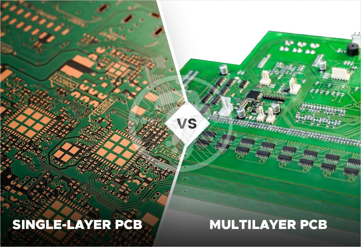
Single-Sided Circuit Boards
Single-sided circuit boards have components and conductive traces on only one side of the board. They are simple and cost-effective, often used in basic electronics like calculators or LED lighting. When assembling these boards with a machine, the focus is on accurate placement and soldering on a single plane, which simplifies the process.
Multi-Layered Boards
Multi-layered boards consist of multiple layers of conductive traces separated by insulating material. They are used in complex devices like smartphones and computers, where space is limited, and high-density interconnects are needed. Assembling these boards requires advanced PCB assembly machines capable of handling intricate designs and ensuring alignment across layers.
Through-Hole Components
Through-hole components have leads that pass through holes in the PCB and are soldered on the opposite side. They are durable and often used in applications requiring strong mechanical connections, such as power supplies. Machine assembly for through-hole components typically involves wave soldering, where a wave of molten solder flows over the board to secure the leads.
Surface-Mounted Components
Surface-mounted components (SMCs) are placed directly onto the surface of the PCB without leads passing through holes. They are smaller and allow for compact designs, making them common in modern electronics. PCB assembly machines for SMCs use pick-and-place technology to position components precisely before soldering, often via a reflow oven.
Essential Tools and Machines for PCB Assembly
To assemble a PCB using a machine, you'll need a set of specialized tools and equipment. Here's a breakdown of the essentials for a professional setup:
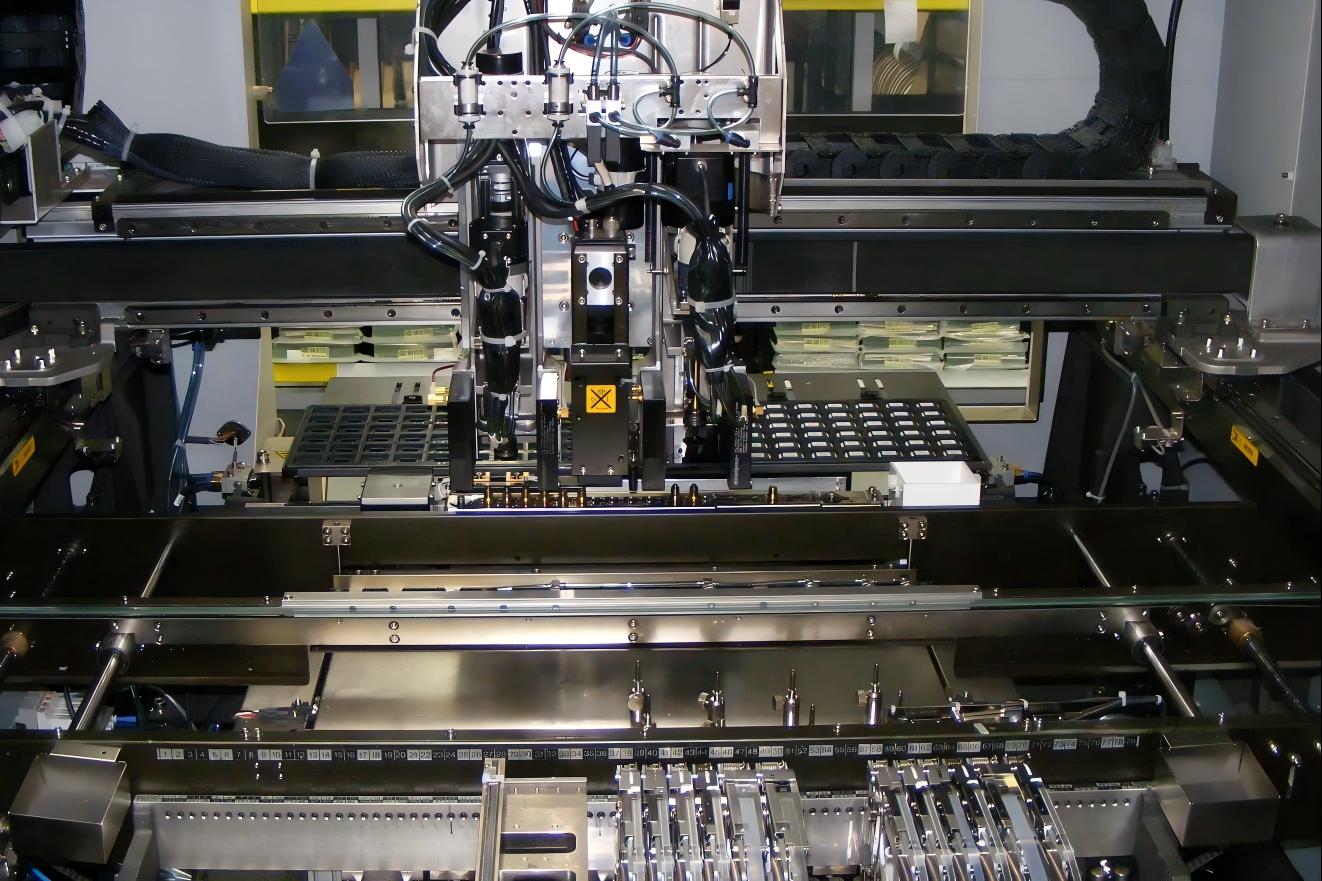
- Pick-and-Place Machine: Automates the placement of surface-mounted components on the PCB with high precision, often handling thousands of components per hour.
- Stencil Printer: Applies solder paste to the PCB through a stencil, ensuring accurate paste deposition for surface-mounted components.
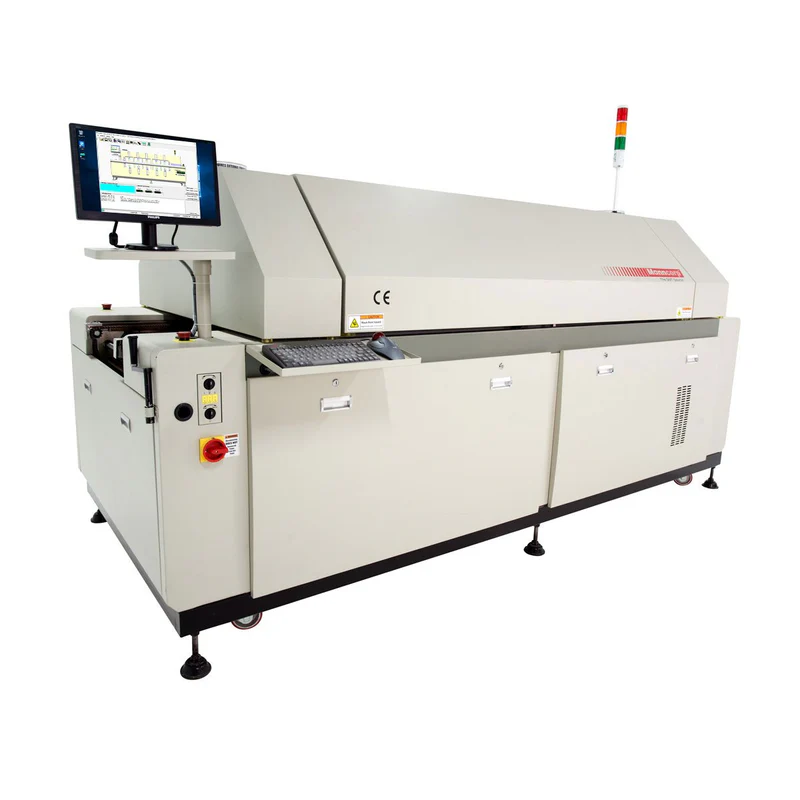
- Reflow Oven: Heats the PCB to melt solder paste, securing surface-mounted components in place during the reflow soldering process.
- Wave Soldering Machine: Used for through-hole components, where a wave of molten solder passes over the board to create strong connections.
- Automated Optical Inspection (AOI) Machine: Inspects the assembled PCB for defects like misaligned components or soldering issues using cameras and software.
- Soldering Iron (Backup): For manual touch-ups or rework on specific components after machine assembly.
Investing in a high-quality PCB assembly machine setup ensures efficiency and reliability, especially for large-scale production or complex designs involving multi-layered boards.
Step-by-Step Guide to PCB Assembly Using a Machine
Now that you understand the types of PCBs and the necessary equipment, let's walk through the detailed process of assembling a PCB using a machine. This guide covers both surface-mounted and through-hole components, ensuring applicability to various projects.
Step 1: Design and Preparation
Every PCB assembly begins with a well-thought-out design. Use reliable design software to create a schematic and layout for your PCB. Ensure that the design accounts for component placement, trace routing, and layer alignment, especially for multi-layered boards. Once the design is finalized, generate Gerber files and a Bill of Materials (BOM) to guide the assembly process.
Preparation also involves setting up the PCB assembly machine. Load the design data into the machine's software to program component placement and soldering patterns. Verify that all components listed in the BOM are available and compatible with the machine's capabilities.
Step 2: Solder Paste Application for Surface-Mounted Components
For PCBs with surface-mounted components, start by applying solder paste using a stencil printer. The stencil, aligned precisely with the PCB, allows solder paste to be deposited only on the pads where components will be placed. This step is critical for ensuring strong and accurate soldering during the reflow process.
Step 3: Component Placement with a Pick-and-Place Machine
Load the PCB into the pick-and-place machine, which uses robotic arms or vacuum nozzles to pick components from reels or trays and place them onto the board. The machine follows the programmed design to position each component with precision, often achieving placement rates of up to 100,000 components per hour in industrial settings. This step is essential for both single-sided circuit boards and complex multi-layered boards.
Step 4: Reflow Soldering for Surface-Mounted Components
After component placement, move the PCB into a reflow oven. The oven heats the board through controlled temperature zones, melting the solder paste to form permanent connections between components and pads. Typical peak temperatures range from 240°C to 260°C, depending on the solder type (e.g., lead-free solder requires higher temperatures). Cooling zones then solidify the solder, completing the process.
Step 5: Wave Soldering for Through-Hole Components
For PCBs with through-hole components, insert the component leads into the designated holes on the board. This can be done manually or with an automated insertion machine for larger runs. Then, pass the PCB through a wave soldering machine, where a wave of molten solder (typically at 260°C) flows over the bottom of the board, securing the leads. Excess solder is removed, and the board cools to finalize the connections.
Step 6: Inspection and Quality Control
After soldering, inspect the PCB for defects using an Automated Optical Inspection (AOI) machine. The AOI scans the board for issues like misaligned components, insufficient solder, or short circuits. For critical applications, additional testing like X-ray inspection may be used to check internal connections in multi-layered boards. Address any identified issues through manual rework if necessary.
Step 7: Functional Testing
Finally, perform functional testing to ensure the assembled PCB operates as intended. Connect the board to a power source and test key functionalities based on the design specifications. For example, measure signal integrity to ensure impedance values match the design (e.g., 50 ohms for high-speed signals). If the board passes all tests, it's ready for integration into the final product.
Innovations in PCB Assembly: 3D Printing in PCB Design
The world of PCB assembly is evolving with new technologies, and 3D printing is at the forefront of this transformation. Traditionally, PCBs are manufactured using subtractive methods, where material is removed to create traces and layers. However, 3D printing offers an additive approach, building PCBs layer by layer with conductive and insulating materials.
3D printing in PCB design allows for rapid prototyping and customization, especially for complex multi-layered boards. It enables engineers to create intricate geometries and embed components directly into the board during printing. This innovation reduces production time and material waste, making it a game-changer for small-batch production or experimental designs.
For instance, conductive inks can be used in 3D printers to print traces with resistances as low as 0.1 ohms per square, suitable for low-power applications. While 3D-printed PCBs are not yet mainstream for high-volume production, they are gaining traction in research and development settings.
Tips for Successful PCB Assembly with Machines
To maximize the efficiency and quality of your PCB assembly process, consider these practical tips:
- Regular Machine Calibration: Ensure your PCB assembly machine is calibrated regularly to maintain placement accuracy within 0.01mm, critical for surface-mounted components.
- Component Verification: Double-check component specifications in the BOM to avoid mismatches, especially for multi-layered boards with tight tolerances.
- Temperature Control: Monitor reflow and wave soldering temperatures to prevent thermal damage to components or boards. Use profiles tailored to your solder type.
- Clean Work Environment: Keep the assembly area free of dust and contaminants to avoid defects during solder paste application or component placement.
- Documentation: Maintain detailed records of each assembly run, including machine settings and inspection results, to troubleshoot issues and improve future processes.
Common Challenges in PCB Assembly and How to Overcome Them
Even with a PCB assembly machine, challenges can arise during the process. Here are some common issues and solutions:
- Tombstoning of Components: Small surface-mounted components may lift on one side during reflow soldering due to uneven heating. Solve this by optimizing the reflow temperature profile to ensure balanced heating.
- Solder Bridges: Excess solder can create unintended connections between pads. Use precise stencil designs and inspect boards with AOI to detect and correct bridges early.
- Misalignment in Multi-Layered Boards: Layer misalignment can disrupt signal integrity. Use high-precision machines and verify design files to ensure accurate layer registration.
- Component Damage: Overheating during soldering can damage sensitive components. Adhere to recommended temperature limits and use thermal relief pads in the design.
Conclusion: Mastering PCB Assembly with Machines
Assembling a Printed Circuit Board using a PCB assembly machine is a powerful way to achieve precision, speed, and reliability in electronics manufacturing. From single-sided circuit boards to complex multi-layered boards, and from through-hole components to surface-mounted components, the right machine setup can handle a wide range of projects. By following the step-by-step guide outlined above and embracing innovations like 3D printing in PCB design, you can elevate your assembly process to meet modern demands.
At ALLPCB, we are committed to supporting your journey in PCB assembly with resources, expertise, and cutting-edge solutions. Whether you're a hobbyist or a professional engineer, mastering machine assembly opens doors to creating high-quality electronic products efficiently. Keep refining your skills, stay updated with emerging technologies, and watch your projects come to life with flawless precision.