 ALLPCB


In the fast-paced world of printed circuit board (PCB) manufacturing, achieving precise solder paste deposition is critical for high-quality surface mount technology (SMT) assemblies. The stencil, a seemingly simple tool, plays a pivotal role in ensuring reliable solder joints, minimizing defects, and boosting production efficiency. At the heart of this process lies stencil aperture design—a complex balance of material selection, thickness, aperture size, and shape that directly impacts solder paste application. In this blog, we explore the key principles of stencil aperture design, offering practical insights for engineers to optimize their SMT processes.
Whether you're prototyping a new design or scaling up for high-volume production, understanding how to tailor aperture designs to your PCB's requirements can make or break your assembly outcomes. Let's dive into the critical factors that ensure optimal solder paste deposition and how to avoid common pitfalls.
Why Stencil Aperture Design Matters
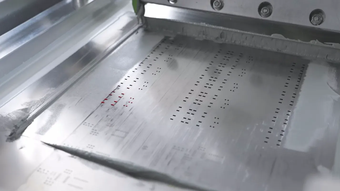
The solder paste stencil is the gateway to accurate and repeatable solder paste deposition in SMT assembly service. Its apertures—precisely cut openings in a thin metal sheet—determine the volume, shape, and placement of solder paste on PCB pads. Poorly designed apertures can lead to defects like solder bridging, insufficient solder joints, or tombstoning, which compromise the reliability of the final product. According to industry data, up to 60-70% of soldering defects stem from issues in the solder paste printing process, underscoring the importance of getting aperture design right.
A well-designed stencil ensures that the right amount of solder paste is applied to each pad, facilitating strong electrical and mechanical connections during reflow soldering. For engineers, this means balancing factors like stencil thickness, aperture size, and shape to match the specific components and PCB layout. Let's break down the key considerations for effective aperture design.
Key Factors in Stencil Aperture Design
1. Stencil Thickness
The thickness of the stencil is one of the most critical factors in determining the volume of solder paste deposited. Thicker stencils deposit more paste, which is suitable for larger components like 1206 resistors or connectors, while thinner stencils are ideal for fine-pitch components like 0201 chips or ball grid arrays (BGAs). Common stencil thicknesses range from 0.08 mm to 0.15 mm, with 0.12 mm being a standard choice for many applications.
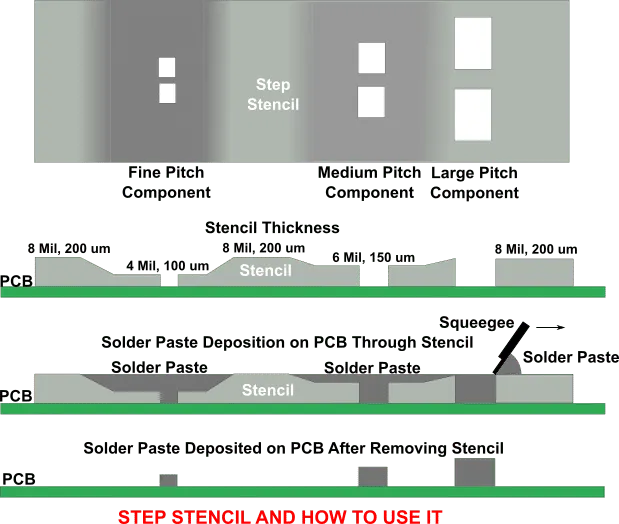
For example, a 0.10 mm stencil is often used for 0201 components to prevent excessive paste that could lead to bridging, while a 0.15 mm stencil might be chosen for larger components requiring more solder volume. However, using a single thickness for a board with diverse components can be challenging. In such cases, stepped stencils—where specific areas are thicker or thinner—can provide tailored paste volumes. Be cautious, though: stepped areas can cause uneven squeegee pressure, potentially leading to inconsistent deposits if apertures are too close to the step edge.
Suggested Reading: The Impact of Stencil Thickness on Solder Joint Quality: A Detailed Analysis
2. Aperture Size and Shape
Aperture size directly influences the amount of solder paste transferred to the PCB. As a general rule, apertures should be slightly smaller than the corresponding PCB pad—typically 10% smaller—to prevent solder paste from spreading beyond the pad and causing bridging. For fine-pitch components like 0.4 mm pitch QFPs, aperture width may need to be reduced to 85% of the pad size, while length can be extended to 110% to ensure adequate paste coverage.
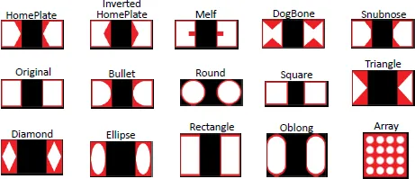
Aperture shape also plays a role. Rectangular and circular apertures are most common, but specialized shapes like home-plate or inverse home-plate are used for small chip components (e.g., 0402) to control paste volume and reduce solder bead formation. For BGAs, circular apertures are often reduced by 0.05 mm compared to pad size for pitches greater than 1.0 mm, while ceramic BGAs may require slightly larger apertures (0.05-0.08 mm) to account for thermal expansion differences.
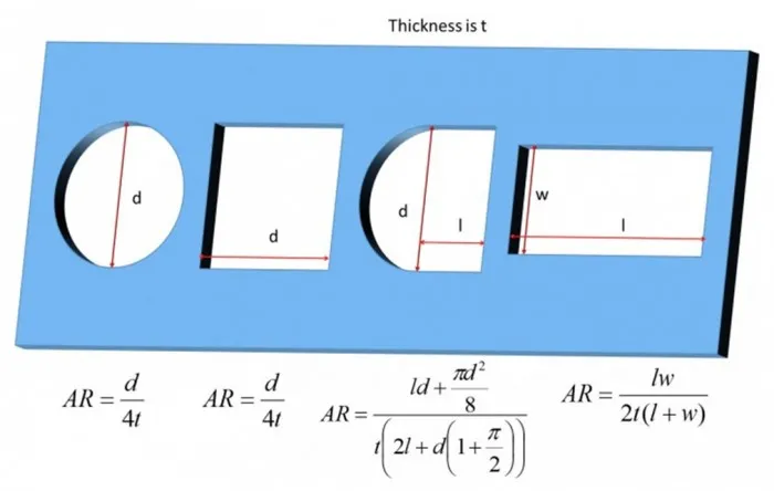
3. Aspect and Area Ratios
To ensure proper solder paste release, two key ratios must be considered: the aspect ratio and the area ratio. The aspect ratio, defined as the aperture width divided by stencil thickness (W/T), should be at least 1.5. The area ratio, calculated as the aperture area divided by the surface area of the aperture walls ((L × W) / [2 × (L + W) × T]), should be at least 0.66. These ratios ensure that the solder paste releases cleanly from the aperture onto the PCB pad, rather than sticking to the aperture walls due to surface tension.
For example, a 0.4 mm wide aperture in a 0.12 mm thick stencil yields an aspect ratio of 3.33 (0.4 / 0.12), which is well above the minimum threshold. However, for ultra-fine-pitch components, laser-cut stencils with electropolished walls can achieve aspect ratios as low as 1.1, improving paste transfer efficiency.
4. Stencil Material and Fabrication Method
Stencils are typically made from stainless steel or nickel due to their durability and precision. Stainless steel is the most common choice for its robustness and cost-effectiveness, while nickel is used in high-density applications for its smoother aperture walls. Fabrication methods include:
- Laser Cutting: Offers high precision and trapezoidal aperture walls, which improve paste release. It's ideal for fine-pitch components and complex designs but may introduce a slight heat-affected zone.
- Chemical Etching: Cost-effective for larger apertures but less precise, making it unsuitable for fine-pitch applications below 0.5 mm.
- Electroforming: Produces ultra-smooth, tapered aperture walls for high-density boards, but it's more expensive and suited for high-volume production.
Electropolishing or micro-plating can further enhance aperture wall smoothness, improving paste transfer efficiency (PTE). PTE, defined as the ratio of deposited paste volume to the theoretical aperture volume, should approach 1 for optimal results. Laser-cut stainless steel stencils with electropolished walls typically achieve PTE values of 0.8 or higher, especially for fine-pitch components like QFNs and BGAs.
5. Alignment and Fiducial Marks
Precise alignment between the stencil and PCB is critical to ensure solder paste is deposited accurately on the pads. Fiducial marks—small, distinct features on the PCB and stencil—serve as alignment references for automated stencil printers. These marks are typically circular or cross-shaped and are included in the PCB's Gerber files. Misalignment, even by a few microns, can result in paste deposition errors, leading to defects like solder bridges or open circuits.
For double-sided PCBs, alignment becomes even more critical. Using a single stencil for both sides can simplify the process, but the stencil design must account for component orientation to minimize tombstoning, where components lift during reflow due to uneven heating.
Best Practices for Aperture Design
To optimize stencil aperture design, engineers should follow these best practices:
- Adhere to IPC-7525 Standards: Ensure aperture designs meet IPC-7525 guidelines for aspect and area ratios to achieve reliable paste transfer.
- Customize for Component Types: Adjust aperture size and shape based on component pitch and type. For example, reduce aperture size by 10-20% for fine-pitch components to prevent bridging.
- Consider Solder Paste Properties: The viscosity and particle size of the solder paste affect deposition. Finer-grain pastes (e.g., Type 4 or 5) are better for smaller apertures, while SAC305 alloys are standard for lead-free soldering.
- Use Trapezoidal Apertures: Laser-cut stencils with trapezoidal apertures (wider at the bottom) improve paste release by reducing surface tension.
- Regular Cleaning and Inspection: Clean stencils after each use with isopropyl alcohol (IPA) or automated cleaning systems to prevent paste residue buildup, which can clog apertures and degrade print quality. Inspect for wear or damage to maintain consistency.
Common Challenges and Solutions
Solder Bridging
Solder bridging occurs when excess paste connects adjacent pads, often due to oversized apertures or excessive stencil thickness. To prevent this, reduce aperture size by 10-20% compared to the pad size and ensure the area ratio exceeds 0.66. For fine-pitch components, consider using electropolished laser-cut stencils to improve paste release.
Insufficient Solder
Insufficient solder paste can lead to weak joints or non-wetting. This often results from undersized apertures or poor paste release due to low area ratios. Increasing aperture size slightly or using a thinner stencil can help. For example, a 0.08 mm stencil may be necessary for 0201 components to ensure adequate paste transfer.
Tombstoning
Tombstoning, where small components stand upright during reflow, can occur due to uneven paste deposition or misalignment. Ensure consistent aperture sizes and proper PCB orientation during printing to balance solder reflow. For double-sided boards, orient components broadside to the direction of travel to ensure simultaneous soldering of both leads.
Suggested Reading: Troubleshooting Common Stencil Printing Defects: A Practical Guide for PCB Assembly
How ALLPCB Supports Optimal Stencil Design
For engineers looking to streamline their SMT assembly process, partnering with a reliable manufacturing service provider is essential. ALLPCB offers high-precision PCB stencils tailored to your specific design requirements, whether for prototyping or high-volume production. Our advanced laser-cutting technology ensures smooth, trapezoidal apertures for optimal paste release, while our quick-turn prototyping services allow you to iterate designs rapidly. With global logistics and a commitment to quality, we help you achieve defect-free assemblies without the hassle of managing complex stencil fabrication in-house.
Conclusion
Stencil aperture design is a critical aspect of SMT assembly that directly impacts the quality and reliability of PCB solder joints. By carefully selecting stencil thickness, aperture size and shape, and fabrication methods, engineers can achieve precise solder paste deposition, minimize defects, and improve manufacturing yields. Adhering to industry standards like IPC-7525, using advanced fabrication techniques like laser cutting, and maintaining proper stencil care are all essential for success.
As PCB design grows more complex with finer pitches and denser layouts, the importance of optimized stencil aperture design will only increase. By following the best practices outlined in this blog and leveraging high-quality manufacturing services, engineers can ensure their assemblies meet the highest standards of performance and reliability.


