 ALLPCB


Solder paste stencil design is a cornerstone of successful printed circuit board (PCB) assembly. For engineers, achieving flawless solder joints means understanding the nuances of stencil design and how it impacts the surface mount technology (SMT) process. A well-designed stencil ensures precise solder paste application, reducing defects like bridging or insufficient solder that can derail a project. In this blog, we dive into the critical factors that shape effective stencil design, offering practical insights to help you optimize your PCB printing process.
Whether you're prototyping a new design or scaling up for production, mastering stencil design can make or break your assembly outcomes. Let's explore the key elements that drive perfection in PCB printing and how you can leverage them to elevate your projects.
Why Solder Paste Stencil Design Matters
Solder paste stencils act as the blueprint for depositing solder paste onto PCB pads, directly influencing the quality of solder joints. Poor stencil design can lead to uneven paste application, causing issues like solder mask bridge, tombstoning, or weak connections that fail under stress. In contrast, a thoughtfully designed stencil ensures consistent paste volume and placement, critical for reliable electrical and mechanical performance.
The stakes are high in modern electronics, where components are shrinking—think 0201 resistors or 0.4mm-pitch BGAs—and tolerances are tighter than ever. A stencil that's off by even 10% in aperture size can disrupt paste release, leading to costly rework. By prioritizing stencil design, you set the stage for efficient assembly and robust circuit performance.
Key Factors in Solder Paste Stencil Design
To achieve perfect PCB printing, several design factors must align. Below, we break down the most critical elements, with actionable tips to guide your approach.
1. Stencil Material Selection
The material of your stencil affects its durability, precision, and cost. Stainless steel is the industry standard due to its strength and resistance to wear, making it ideal for high-volume production runs. For instance, a 0.1mm-thick stainless steel stencil can handle thousands of prints without deforming, ensuring consistency across batches.
Nickel stencils, while pricier, offer superior paste release for fine-pitch components (e.g., 0.3mm pitch QFPs) thanks to their smoother aperture walls. Polyimide stencils, on the other hand, are a cost-effective choice for prototypes, though they're less durable and better suited for low-volume runs of simpler boards.
Tip: Choose stainless steel for production runs exceeding 500 boards, but consider polyimide for one-off prototypes to save on costs.
2. Stencil Thickness
Stencil thickness determines the volume of solder paste deposited, which must match the component requirements. Common thicknesses range from 0.05mm to 0.2mm. Thinner stencils (e.g., 0.08mm) are ideal for small components like 0402 resistors, delivering less paste to prevent bridging. Thicker stencils (e.g., 0.15mm) suit larger components like 1206 capacitors, ensuring enough paste for strong joints.
A mismatch in thickness can cause havoc. For example, using a 0.2mm stencil for a 0.5mm-pitch BGA might deposit too much paste, leading to solder balls that short circuits. Conversely, a too-thin stencil for a QFN package could starve the joint, compromising mechanical strength.
Tip: Use the aspect ratio (aperture width divided by stencil thickness) to guide thickness choice. Aim for an aspect ratio above 1.5 for reliable paste release.
Suggested Reading: The Impact of Stencil Thickness on Solder Joint Quality: A Detailed Analysis
3. Aperture Design and Size
Aperture design is where precision meets practicality. Apertures are the holes in the stencil that allow solder paste to flow onto PCB pads, and their size and shape must align with the pad layout. A general rule is to make apertures 10-20% smaller than the pad to prevent overspreading, which can cause bridging. For a 1mm x 1mm square pad, an aperture of 0.8mm x 0.8mm is a safe starting point.
For fine-pitch components, trapezoidal apertures—wider at the bottom—improve paste release by reducing clogging. The area ratio (aperture area divided by wall area) should exceed 0.66 to ensure clean paste transfer. For instance, a 0.4mm circular aperture in a 0.1mm-thick stencil needs careful design to avoid paste sticking in the hole.
Tip: For BGAs, use square or rounded-square apertures to match ball shapes, and reduce aperture size by 15% for pitches below 0.5mm to minimize defects.
Suggested Reading: Stencil Aperture Design for Optimal Solder Paste
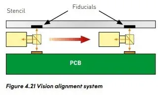
4. Fiducial Marks for Alignment
Alignment is non-negotiable in stencil printing. Fiducial marks—small, distinct features on the PCB and stencil—enable precise positioning, especially in automated printers. Without them, misalignment by even 0.05mm can shift paste deposits, leading to misaligned components.
Place at least three global fiducials on the board's edges, each 1-3mm in diameter, with a 3mm clearance from other features. For complex boards with fine-pitch ICs, add local fiducials near critical components to fine-tune alignment.
Tip: Ensure fiducials are etched clearly on both the PCB and stencil, and verify their visibility under your printer's vision system.
5. Squeegee Parameters
The squeegee, which spreads solder paste across the stencil, plays a pivotal role in print quality. Its angle, pressure, and speed must be optimized. A 60-degree angle is standard, balancing paste roll and aperture filling. Too steep (e.g., 70 degrees) can scoop paste out, while too shallow (e.g., 45 degrees) leaves residue.
Pressure should be around 500 grams per 25mm of squeegee length to achieve a clean wipe without damaging the stencil. Speed, typically 25mm per second, affects how paste fills apertures—slower speeds suit fine-pitch designs, while faster speeds work for larger pads.
Tip: Test squeegee settings on a sample board to find the sweet spot, adjusting pressure first, then speed, to avoid smearing or scooping.
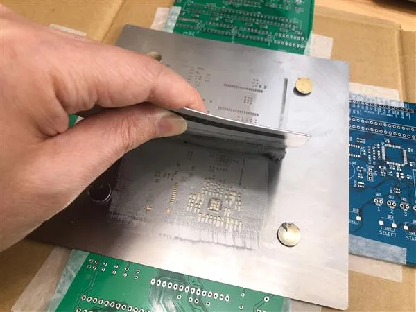
6. Stencil Manufacturing Techniques
How a stencil is made impacts its performance. Laser cutting is the gold standard, offering precision down to 0.05mm for aperture placement, ideal for ultra-fine-pitch components. Electroforming, used for nickel stencils, creates smoother walls but is costlier and reserved for high-end applications like wafer bumping.
Chemical etching, while cheaper, struggles with fine features, often producing rougher edges that trap paste. For a 0.4mm-pitch QFP, laser-cut stainless steel outperforms etched alternatives by delivering cleaner paste deposits.
Tip: Invest in laser-cut stencils for designs with pitches below 0.8mm to ensure accuracy and repeatability.
Common Challenges and How to Overcome Them
Even with a solid design, stencil printing can hit snags. Here are three frequent issues and their fixes:
- Bridging: Caused by excess paste from oversized apertures or high squeegee pressure. Solution: Reduce aperture size by 10% and lower pressure by 100 grams incrementally.
- Insufficient Paste: Often due to clogged apertures or a too-thin stencil. Solution: Clean the stencil after every 10 prints and verify thickness matches component needs.
- Misalignment: Results from poor fiducial detection or board warpage. Solution: Add local fiducials and use a vacuum holder to secure the PCB.
Regular stencil cleaning—manual or automatic—prevents residue buildup, especially for fine-pitch designs. A quick wipe with isopropyl alcohol every few prints keeps apertures clear.
Suggested Reading: Troubleshooting Common Stencil Printing Defects: A Practical Guide for PCB Assembly
Advanced Considerations for Complex Designs
For HDI PCB with mixed components, standard stencils may fall short. Step stencils, with varying thicknesses (e.g., 0.1mm for 0402s and 0.15mm for connectors), allow tailored paste volumes on a single board. These are pricier but essential for designs with diverse pad sizes.
Nano-coatings, like hydrophobic films, enhance paste release for ultra-fine apertures (e.g., 0.3mm pitch). They're overkill for simple boards but a game-changer for complex assemblies, reducing defects by up to 20% in some studies.
Tip: Evaluate step stencils for boards with both fine-pitch ICs and large power components to balance paste requirements without compromising quality.

Best Practices for Stencil Printing Success
To tie it all together, follow these best practices:
1. Validate Design Early: Use PCB design software to simulate paste deposition and catch aperture issues before manufacturing.
2. Test with Prototypes: Print a few boards to tweak squeegee settings and confirm alignment.
3. Monitor Paste Condition: Store solder paste at 4-10°C and mix it thoroughly before use to maintain viscosity.
4. Inspect Post-Print: Use solder paste inspection (SPI) to verify volume and alignment, catching defects early.
5. Maintain Stencils: Clean regularly and store flat in antistatic packaging to prevent damage.
By integrating these steps, you'll minimize rework and boost assembly yields, even on challenging designs.
How ALLPCB Supports Your Stencil Design Needs
When it comes to turning your stencil designs into reality, we at ALLPCB are here to help. Our advanced manufacturing capabilities deliver laser-cut stencils with precision down to 0.05mm, perfect for fine-pitch and high-density boards. With quick-turn prototyping, we can produce your stencil in as little as 24 hours, keeping your project on track. Our global logistics ensure fast delivery, whether you're building a single prototype or scaling up for production. Plus, our team offers design assistance to optimize aperture layouts, helping you achieve flawless prints every time.
Conclusion: Elevate Your PCB Printing with Smart Stencil Design
Solder paste stencil design is more than a technical step—it's the foundation of reliable PCB assembly. By focusing on material, thickness, aperture design, alignment, and printing parameters, you can achieve consistent, high-quality results that stand up to the demands of modern electronics. Whether you're tackling a prototype or a production run, these factors empower you to minimize defects and maximize performance.
Take the time to refine your stencil design process, test your setups, and leverage advanced techniques like step stencils or nano-coatings when needed. With the right approach, you'll turn complex PCB layouts into robust, functional boards that deliver every time.


