 ALLPCB


Are you struggling with overheating issues on your printed circuit board (PCB)? Hotspots can lead to performance drops, component failure, or even complete system breakdowns. In this comprehensive guide, we’ll dive into PCB hotspot troubleshooting, explore common thermal via problems, and provide actionable steps for diagnosing overheating, PCB repair, and improving thermal performance. Whether you're a seasoned engineer or a hobbyist, this post will equip you with the tools and knowledge to tackle thermal challenges effectively.
Let’s be with ALLPCB to break down the process of identifying and resolving thermal issues on your PCB, ensuring your designs run cooler and last longer. From understanding the role of thermal vias to practical repair tips, we’ve got you covered with detailed insights and strategies.
Why Thermal Management Matters in PCB Design
Thermal management is a critical aspect of PCB design. As electronic devices become smaller and more powerful, the heat generated by components increases significantly. Without proper heat dissipation, temperatures can rise beyond safe limits—often exceeding 85°C for many components—leading to reduced lifespan, erratic behavior, or catastrophic failure. For high-power applications, such as power supplies or LED drivers, effective thermal management can mean the difference between a reliable product and a costly redesign.
Hotspots, or localized areas of excessive heat, are often the root cause of thermal issues. These can result from poor component placement, inadequate heat sinking, or ineffective use of thermal vias. Addressing these problems early through PCB hotspot troubleshooting can save time and resources in the long run.
What Are Thermal Vias and Why Do They Matter?
Thermal vias are small, plated holes in a PCB that transfer heat from one layer to another, often connecting heat-generating components to a ground plane or heat sink on the opposite side. They act as conduits for heat, helping to distribute it evenly across the board and prevent localized overheating. Typically, thermal vias are placed directly under or near high-power components like power transistors or microcontrollers.
However, thermal via problems can undermine their effectiveness. Issues such as insufficient via count, improper placement, or poor connection to heat-dissipating layers can lead to hotspots. For instance, a thermal via with a diameter of 0.3 mm may only handle a small amount of heat transfer, whereas increasing the diameter to 0.5 mm or adding more vias can improve performance by up to 30%, depending on the design.
Understanding how thermal vias work and where they might fail is the first step in diagnosing overheating issues on your PCB. Let’s explore how to spot these problems and fix them.
Common Causes of PCB Hotspots and Overheating
Before diving into troubleshooting, it’s essential to understand the common causes of overheating on PCBs. Identifying the root cause will help you apply the right fix and prevent future issues.
- Insufficient Thermal Vias: If there aren’t enough vias or they’re too small, heat can’t escape efficiently. For example, a high-power component dissipating 5W of heat might require at least 10-15 vias with a 0.4 mm diameter for adequate dissipation.
- Poor Component Placement: Placing heat-generating components too close together can create concentrated hotspots. Spacing components at least 5-10 mm apart in high-power designs can reduce thermal overlap.
- Inadequate Copper Planes: Copper layers act as heat spreaders, but if they’re too thin (e.g., 1 oz instead of 2 oz) or disconnected from vias, heat remains trapped.
- Blocked Airflow: Enclosed designs or poor ventilation can trap heat, raising temperatures by 10-20°C above ambient levels.
- Overloaded Components: Running components beyond their rated power or current—such as a MOSFET handling 10A when rated for 8A—can cause excessive heat buildup.
These issues often compound each other, making diagnosing overheating a complex but necessary task. Let’s move on to how you can identify hotspots and thermal via problems in your design.
Step-by-Step Guide to Diagnosing Overheating on Your PCB
Finding and addressing hotspots requires a systematic approach. Here’s a step-by-step guide to PCB hotspot troubleshooting and diagnosing thermal issues.
1. Visual Inspection
Start with a close examination of your PCB. Look for signs of overheating, such as discoloration of the board material (often turning brown or black), burnt components, or melted solder joints. These are clear indicators of thermal stress, often localized around specific components or areas with poor heat dissipation.
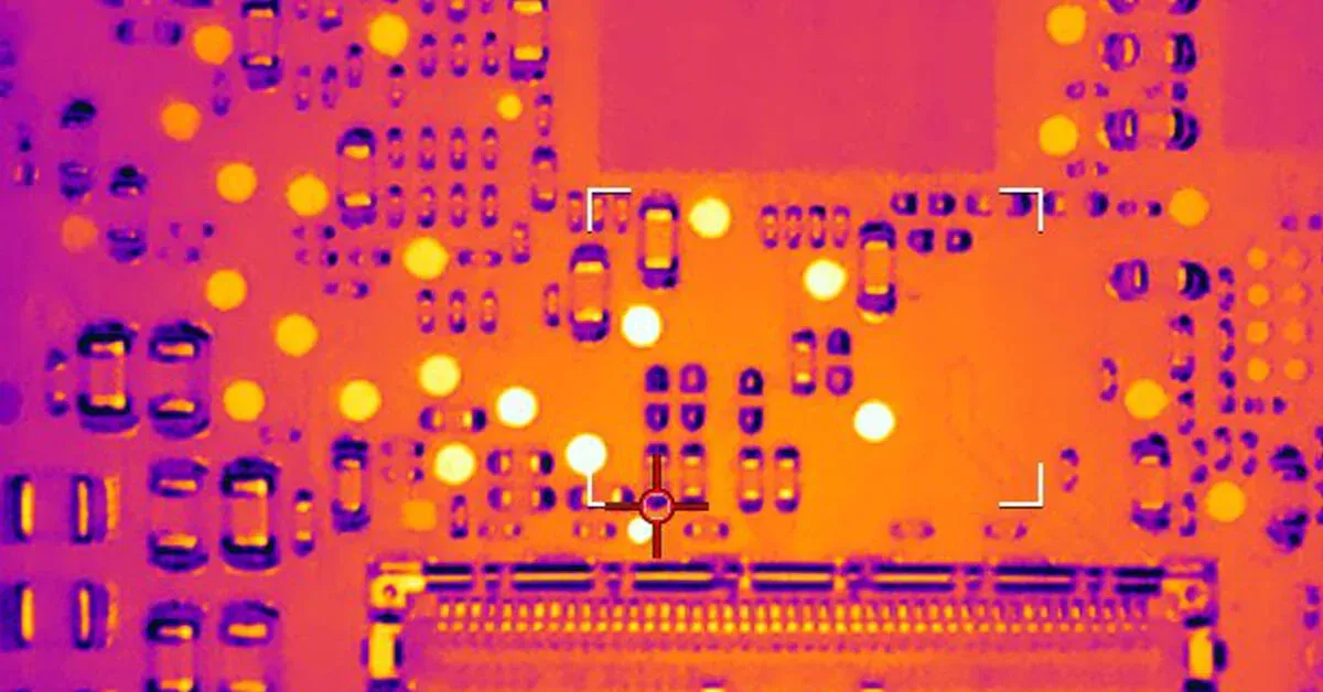
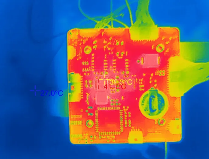
2. Use a Thermal Camera
A thermal imaging camera is an invaluable tool for identifying hotspots. These devices can detect temperature differences as small as 0.1°C, allowing you to visualize heat distribution across the board. Focus on areas around high-power components and thermal vias. Temperatures exceeding 100°C often signal a problem that needs immediate attention.
3. Measure Component Temperatures
If a thermal camera isn’t available, use a contact thermometer or infrared thermometer to measure the temperature of specific components. Compare these readings against the manufacturer’s maximum operating temperature (often listed in datasheets as 85°C or 125°C for most ICs). Consistent readings above these limits indicate a thermal issue.
4. Check Thermal Via Effectiveness
Inspect the placement and condition of thermal vias. Are they directly under heat-generating components? Are they connected to a large copper plane or heat sink? Use a multimeter to check for continuity between vias and ground planes to ensure proper connection. Poorly connected vias or those filled with solder can reduce heat transfer by up to 50%.
5. Simulate Heat Dissipation
For a more advanced diagnosis, use PCB design software with thermal simulation capabilities. These tools can predict heat distribution based on your layout and component power ratings. For instance, a simulation might reveal that a particular area reaches 110°C due to insufficient vias, guiding you to add more or increase copper thickness.
By following these steps, you can pinpoint the source of overheating and move on to effective solutions for PCB repair and thermal management.
Solutions for Fixing Thermal Via Problems and Hotspots
Once you’ve identified the cause of overheating, it’s time to implement solutions. Here are proven strategies for addressing thermal via problems and improving thermal performance.
1. Optimize Thermal Via Design
Increase the number and size of thermal vias under high-power components. As a rule of thumb, aim for a via density of 1 via per 1-2 mm2 of pad area for components dissipating more than 2W. Use vias with a diameter of at least 0.3-0.5 mm to maximize heat transfer. Additionally, ensure vias are connected to thick copper layers (2 oz or higher) for better heat spreading.
Suggested Reading: Optimizing Thermal Vias for SMT Components: A Step-by-Step Guide
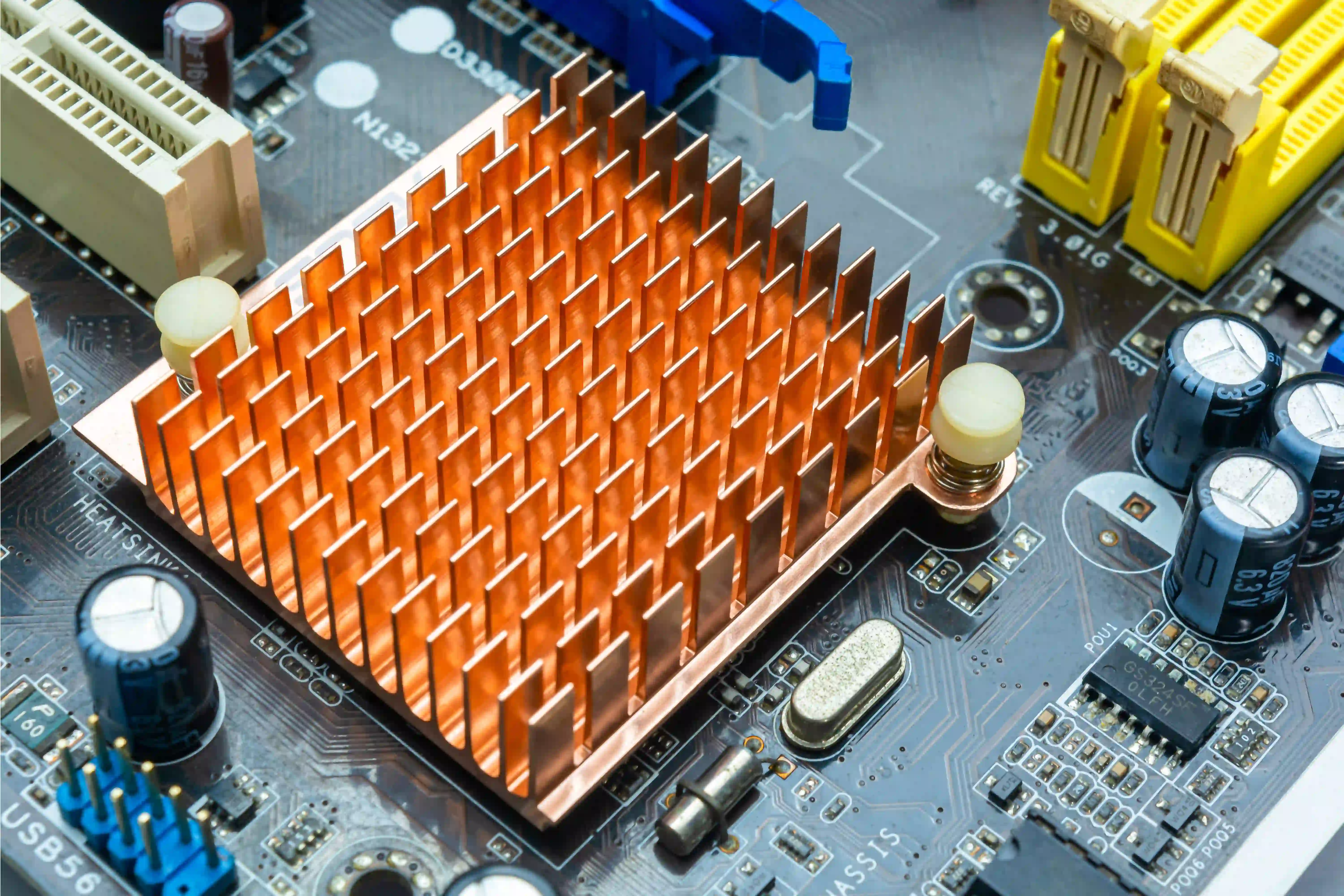
2. Add Heat Sinks or Thermal Pads
For components generating significant heat, attach heat sinks directly to the component or through thermal vias to a copper plane. Thermal pads or compounds can improve contact and reduce thermal resistance by up to 20%. For example, a heat sink rated for 5W dissipation can lower component temperatures by 15-25°C in typical conditions.
3. Improve Component Placement
Redesign your layout to space out heat-generating components. Avoid clustering high-power devices in one area, and place them near board edges or ventilation slots if possible. This can reduce localized temperatures by 10-15°C, based on typical airflow patterns in enclosures.
4. Enhance Copper Layers
Increase the thickness of copper planes or add more layers dedicated to heat dissipation. A 2 oz copper layer can handle approximately twice the thermal load of a 1 oz layer. Connect these planes to thermal vias to create a robust heat dissipation network across the board.
5. Incorporate Active Cooling
For high-power designs, passive cooling may not suffice. Adding small fans or active cooling solutions can reduce temperatures by 20-30°C. Ensure the fan’s airflow aligns with the PCB layout to target hotspot areas effectively.
PCB Repair Tips for Overheating Damage
If overheating has already caused damage, PCB repair is often necessary. Here’s how to address common issues caused by thermal stress.
- Replace Damaged Components: Overheated components like capacitors or resistors may fail or show reduced performance. Use a soldering iron to carefully desolder and replace them with parts rated for higher temperatures if possible.
- Fix Solder Joints: Heat can crack or weaken solder joints. Reflow these joints with fresh solder to restore connectivity, ensuring the joint temperature doesn’t exceed 260°C during rework to avoid further damage.
- Repair Traces: Overheating can delaminate or burn PCB traces. Use conductive epoxy or jumper wires to bridge damaged sections, then test for continuity with a multimeter.
After repairs, retest the board under load to confirm that temperatures remain within safe limits (below 85°C for most components). If issues persist, consider a full redesign with the thermal management strategies discussed earlier.
Preventing Future Thermal Issues in PCB Design
Prevention is always better than repair. Here are proactive steps to ensure your future designs avoid thermal via problems and overheating.
- Plan Thermal Management Early: During the schematic and layout phase, identify high-power components and allocate space for thermal vias and heat sinks. Use design rules to enforce minimum via counts based on power dissipation.
- Use High-Quality Materials: Opt for PCB substrates with better thermal conductivity, such as FR-4 with enhanced thermal properties or metal-core boards for extreme cases. These can improve heat dissipation by up to 40% compared to standard materials.
- Test Under Real Conditions: After assembly, test your PCB under full load in its intended environment. Monitor temperatures over extended periods (e.g., 24 hours) to catch intermittent thermal issues.
- Iterate Based on Feedback: Use data from thermal testing to refine your design. If a particular area consistently overheats, adjust via placement or add cooling solutions before final production.
Conclusion: Mastering PCB Thermal Performance
Dealing with PCB hotspots and overheating can be challenging, but with the right approach to PCB hotspot troubleshooting, you can diagnose and fix issues effectively. By addressing thermal via problems, using tools like thermal cameras for diagnosing overheating, and applying strategies for PCB repair, you’ll ensure your boards operate reliably under demanding conditions. Moreover, incorporating best practices for improving thermal performance in your designs will prevent future issues and extend the lifespan of your electronics.
Thermal management is not just a technical necessity—it’s a cornerstone of high-quality PCB design. With the actionable steps and insights provided in this guide, you’re well-equipped to tackle thermal challenges head-on. Keep refining your skills and designs, and your PCBs will perform at their best, no matter the application.


