In the fast-paced world of electronics, designing high-frequency PCBs (Printed Circuit Boards) is a critical task that demands precision and foresight. One of the most important aspects of this process is optimizing PCB trace routing to ensure signal integrity and performance. But how do you achieve this while also focusing on Design for Manufacturability (DFM)? This blog dives deep into a DFM-focused strategy for routing traces in high-frequency PCBs, balancing performance with production efficiency. We’ll explore key concepts like impedance control, trace layout techniques, and practical tips to streamline your design process.
Whether you’re an experienced engineer or just starting with high-frequency designs, this guide will provide actionable insights to help you create reliable, high-performing boards. Let’s break down the essentials of PCB trace routing and how a DFM approach can make a difference.
Why PCB Trace Routing Matters in High-Frequency Designs
High-frequency PCBs operate at signal speeds where even small design flaws can lead to significant issues like signal loss, crosstalk, or electromagnetic interference (EMI). PCB trace routing—the path that electrical signals take across the board—plays a pivotal role in maintaining signal integrity. Poor routing can cause delays, reflections, or noise, which are especially problematic when dealing with frequencies above 100 MHz.
In high-frequency designs, traces act as transmission lines, and their geometry directly impacts impedance. Mismatched impedance can distort signals, leading to data errors in applications like telecommunications, RF systems, or high-speed digital circuits. Additionally, manufacturability is a concern. A design that performs well in theory but ignores DFM principles may result in costly production errors or delays.
By focusing on both performance and DFM, you can create a design that not only meets technical requirements but is also easier and more cost-effective to produce. Let’s explore how to achieve this balance.
Key Challenges in High-Frequency PCB Trace Routing
Before diving into solutions, it’s important to understand the unique challenges of routing traces in high-frequency PCBs:
- Signal Integrity: At high frequencies, signals are prone to reflections and crosstalk if traces are not properly designed.
- Impedance Matching: Traces must maintain consistent impedance (often 50 ohms for RF designs) to prevent signal distortion.
- EMI and Noise: High-frequency signals can generate or pick up interference, impacting nearby traces or components.
- Thermal Management: High-speed signals can generate heat, requiring careful trace width and spacing to avoid overheating.
- Manufacturing Constraints: Tight tolerances and complex layouts can lead to production issues if DFM isn’t considered.
Addressing these challenges requires a strategic approach that combines electrical design principles with manufacturing know-how. Let’s look at how to optimize trace routing with a DFM focus.
Core Strategies for Optimizing PCB Trace Routing
1. Prioritize Impedance Control in Trace Design
Impedance control is the foundation of high-frequency PCB design. Traces must be designed to match the impedance of the system—commonly 50 ohms for RF or 100 ohms for differential pairs in high-speed digital circuits. To achieve this, consider the following:
- Trace Width and Thickness: Use a trace width calculator to determine the correct dimensions based on the substrate material and dielectric constant. For example, on a standard FR-4 material with a dielectric constant of 4.5, a 50-ohm trace might require a width of around 6 mils for a 1.6mm board.
- Stack-Up Design: Ensure that the PCB layer stack-up supports controlled impedance by placing ground planes close to signal layers. This reduces noise and maintains consistent impedance.
- Material Selection: High-frequency designs often benefit from low-loss materials like Rogers or Teflon, which offer better signal performance compared to standard FR-4 at frequencies above 1 GHz.
From a DFM perspective, ensure that your trace widths and spacing align with the capabilities of your manufacturing partner. Many manufacturers have minimum trace width and spacing limits (often around 4-6 mils for standard processes), so design within these constraints to avoid production issues.
2. Minimize Trace Length and Avoid Sharp Corners
In high-frequency designs, the length of a trace affects signal propagation delay and potential reflections. Keep traces as short as possible to reduce these effects. For critical signals, match trace lengths within a tolerance of 5-10 mils to avoid timing mismatches, especially in differential pairs.
Additionally, avoid sharp 90-degree corners in trace routing. Sharp bends can cause signal reflections due to impedance discontinuities. Instead, use 45-degree angles or smooth curves (often called “arcs”) to maintain signal integrity. Modern design software can automate this process, ensuring consistent routing.
For DFM, minimizing trace length also reduces material usage and simplifies the layout, which can lower production costs. Be mindful of via placement as well—excessive vias can introduce inductance and signal loss, so use them sparingly.
3. Maintain Proper Trace Spacing to Reduce Crosstalk
Crosstalk occurs when signals from one trace interfere with another, a common issue in high-frequency designs. To prevent this, maintain adequate spacing between traces. A general rule is to keep spacing at least three times the trace width (3W rule) for parallel traces to minimize coupling.
For differential pairs, ensure symmetry in routing. Both traces in the pair should have identical lengths and spacing to maintain signal balance. This reduces noise and improves performance in high-speed applications like USB or HDMI.
From a manufacturing standpoint, wider spacing makes etching and inspection easier, reducing the risk of defects. Check with your manufacturer for their minimum spacing capabilities to ensure your design is producible.
4. Use Ground Planes for Signal Reference and Noise Reduction
A solid ground plane is essential in high-frequency PCB designs. It provides a low-impedance return path for signals, reducing EMI and noise. Place a continuous ground plane directly beneath signal layers, and avoid splitting the plane unless absolutely necessary, as splits can disrupt return paths and cause signal issues.
For DFM, a well-designed ground plane simplifies the manufacturing process by reducing the need for complex routing adjustments. It also enhances thermal dissipation, which is a bonus for high-frequency circuits that generate heat.
DFM-Focused Tips for High-Frequency PCB Routing
Design for Manufacturability ensures that your high-frequency PCB design isn’t just functional but also practical to produce. Here are some DFM-focused tips to complement your routing strategy:
- Stick to Standard Trace Widths and Spacing: Use trace widths and spacing that align with common manufacturing capabilities (e.g., 5-6 mils for standard processes). This avoids the need for specialized equipment or processes, which can increase costs.
- Avoid Overly Tight Tolerances: While high-frequency designs often require precision, overly tight tolerances can lead to higher rejection rates during production. Balance performance needs with realistic manufacturing limits.
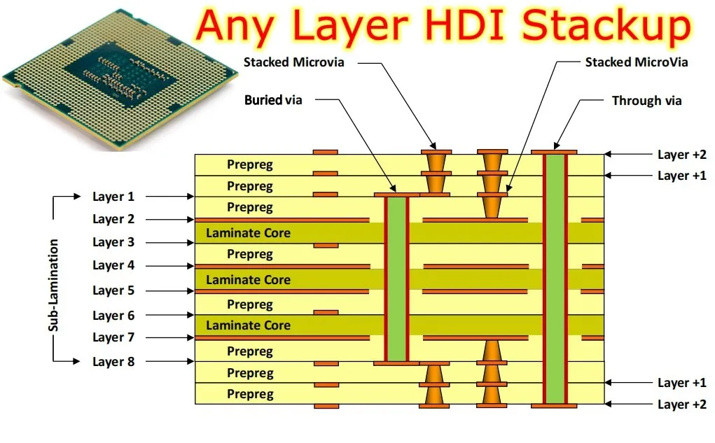
- Optimize Via Usage: Minimize the number of vias in high-frequency signal paths to reduce inductance and signal loss. When vias are necessary, use standard sizes (e.g., 10-12 mils) to ensure compatibility with most fabrication processes.
- Plan for Testing and Inspection: Include test points in your design to facilitate signal integrity testing during production. This can help catch issues early and reduce rework costs.
By incorporating these DFM principles, you ensure that your high-frequency PCB is not only high-performing but also cost-effective and reliable to manufacture.
Tools and Software for Optimizing Trace Routing
Modern PCB design software offers powerful tools to assist with high-frequency trace routing and DFM. These tools can simulate signal behavior, calculate impedance, and highlight potential manufacturing issues before production. Some key features to look for include:
- Impedance Calculators: Built-in tools to determine trace width and spacing for specific impedance values.
- Signal Integrity Analysis: Simulations to predict crosstalk, reflections, and other signal issues.
- DFM Checks: Automated checks for minimum trace widths, spacing, and other manufacturing constraints.
Using these tools during the design phase can save time and prevent costly errors. They also help bridge the gap between electrical performance and manufacturability, ensuring a smoother transition from design to production.
Common Mistakes to Avoid in High-Frequency PCB Routing
Even with the best intentions, certain mistakes can compromise your high-frequency PCB design. Here are some pitfalls to watch out for:
- Ignoring Impedance Mismatch: Failing to match trace impedance to the system requirements can lead to signal reflections and data errors.
- Overusing Vias: Excessive vias in signal paths introduce inductance, degrading performance at high frequencies.
- Neglecting Ground Planes: Skipping or splitting ground planes disrupts return paths, increasing noise and EMI.
- Overlooking DFM Guidelines: Designing without considering manufacturing limits can result in boards that are difficult or expensive to produce.
By being aware of these issues, you can take proactive steps to avoid them and create a more robust design.
Conclusion: Balancing Performance and Manufacturability
Optimizing PCB trace routing in high-frequency PCBs is a delicate balance of electrical performance and Design for Manufacturability. By focusing on impedance control, minimizing trace length, maintaining proper spacing, and using solid ground planes, you can ensure signal integrity in even the most demanding applications. At the same time, adhering to DFM principles like standard trace widths, realistic tolerances, and minimal via usage helps streamline production and reduce costs.
High-frequency PCB design doesn’t have to be a daunting task. With the right strategies and tools, you can create boards that perform reliably while being practical to manufacture. Keep these tips in mind during your next project to achieve the best of both worlds—superior performance and efficient production.
Ready to apply these principles to your next high-frequency PCB design? Start with a clear plan, leverage design software for simulations, and always consider manufacturing constraints from the outset. Your designs will not only meet technical specs but also move smoothly from prototype to production.
 ALLPCB


