 ALLPCB


If you're looking to improve SMT component cooling and prevent overheating in your surface mount PCB designs, optimizing thermal vias is a critical step. Thermal vias help transfer heat away from surface mount technology (SMT) components, ensuring better performance and longer device life. In this comprehensive guide, we'll walk you through the process of thermal via placement for SMT, optimizing via layout, and effective SMT thermal management strategies. Whether you're a beginner or an experienced engineer, this step-by-step approach will help you master surface mount PCB design for efficient heat dissipation.
Why Thermal Vias Matter in SMT Component Cooling
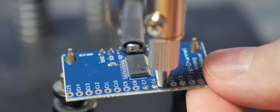
Thermal vias are small, plated holes in a printed circuit board (PCB) that conduct heat away from SMT components to a heat sink or other layers of the board. In modern electronics, SMT components like microcontrollers, power ICs, and LEDs generate significant heat in compact spaces. Without proper SMT component cooling, this heat can cause performance issues, reduce lifespan, or even lead to complete failure.
By strategically placing thermal vias, you can create a direct path for heat to escape, lowering the operating temperature of critical components. Studies suggest that reducing junction temperature by just 10°C can double the lifespan of a semiconductor device. This makes thermal via placement for SMT a non-negotiable aspect of surface mount PCB design.
Understanding the Basics of Thermal Vias in SMT Design
Before diving into the step-by-step guide, let's cover the fundamentals of thermal vias and their role in SMT thermal management. Thermal vias are typically filled or plated with a conductive material like copper to maximize heat transfer. They connect the component's thermal pad (often on the top layer) to a larger copper plane or heat sink on another layer of the PCB.
The effectiveness of thermal vias depends on factors like size, number, placement, and the thermal conductivity of the materials used. For instance, a via with a diameter of 0.3 mm and copper plating can conduct heat at a rate proportional to the thermal conductivity of copper (approximately 400 W/m·K). Understanding these basics is key to optimizing via layout for your design.
Step-by-Step Guide to Optimizing Thermal Vias for SMT Components
Now, let's break down the process of designing and placing thermal vias for effective SMT component cooling. Follow these steps to ensure your surface mount PCB design achieves optimal thermal performance.
Step 1: Identify High-Heat SMT Components
Start by analyzing your schematic and PCB layout to pinpoint components that generate the most heat. Common culprits include power regulators, MOSFETs, and high-current ICs. Check the datasheets for these components to find their maximum junction temperature and thermal resistance values (often listed as θJA, or junction-to-ambient thermal resistance, in °C/W). This data will guide your thermal via strategy for SMT thermal management.
For example, if a power IC has a θJA of 40°C/W and dissipates 2W of power, the temperature rise could be 80°C above ambient without proper cooling. Thermal vias can significantly reduce this rise by providing a low-resistance heat path.
Step 2: Determine Thermal Via Requirements
Next, calculate the number and size of thermal vias needed based on the heat dissipation requirements. A common rule of thumb is to use 8 to 12 vias per square centimeter under a component's thermal pad for moderate heat dissipation. For high-power components dissipating over 5W, you might need 20 or more vias in the same area.
The via diameter also matters. Larger vias (e.g., 0.5 mm) conduct more heat but take up more space and can interfere with signal routing. Smaller vias (e.g., 0.3 mm) are more space-efficient but less effective individually. Balance these factors based on your design constraints.
Step 3: Optimize Thermal Via Placement for SMT
Placement is critical for effective thermal via placement for SMT. Position vias directly under or as close as possible to the thermal pad of the SMT component. This minimizes the thermal resistance path. Avoid placing vias too far from the heat source, as this reduces their effectiveness.
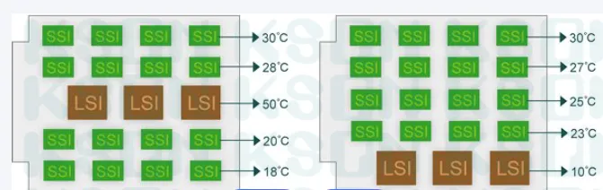
Arrange vias in a grid pattern to evenly distribute heat transfer. For instance, a 3x3 grid under a 9 mm2 thermal pad ensures uniform cooling. If space is limited, prioritize placing vias near the center of the pad, where heat concentration is typically highest.
Also, ensure the vias connect to a large copper plane (often the ground plane) on an inner or bottom layer. A copper plane with an area of at least 10 times the component's thermal pad size can act as an effective heat sink.
Step 4: Connect Vias to Heat Sinks or Copper Planes
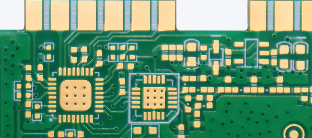
Thermal vias are most effective when connected to a substantial heat-dissipating layer. In multilayer PCBs, route vias to an internal ground plane or a dedicated thermal layer. Ensure the copper plane has minimal interruptions from other traces or components to maximize heat spreading.
For double-sided PCBs, connect vias to a large copper area on the bottom layer. If possible, expose this copper area to air or attach a physical heat sink for additional cooling. A copper thickness of 2 oz (70 μm) or more is ideal for better heat distribution in surface mount PCB design.
Step 5: Consider Via Fill and Plating Options
Standard thermal vias are plated through-holes, but filling them with a conductive material like copper or epoxy can enhance heat transfer. Copper-filled vias offer superior thermal conductivity (up to 400 W/m·K) compared to unfilled vias, but they are more expensive to manufacture. Conductive epoxy fills are a cost-effective alternative, though less efficient (around 5-10 W/m·K).
Weigh the cost versus performance benefits based on your project's needs. For high-power applications, filled vias might be worth the investment for optimal SMT thermal management.
Step 6: Simulate and Test Your Design
Before finalizing your layout, use thermal simulation software to model heat flow in your PCB. Many PCB design softwares offer built-in thermal analysis features that predict temperature rises and identify hotspots. Look for areas where the temperature exceeds the component's safe operating limit (often 85°C to 125°C for most SMT parts).
After manufacturing, test the physical board under real-world conditions. Use an infrared camera or thermocouple to measure the temperature of critical components. If hotspots persist, adjust the number or placement of thermal vias in the next revision.
Best Practices for Optimizing Via Layout in SMT Designs
Beyond the basic steps, here are some advanced tips for optimizing via layout and achieving superior SMT component cooling.
- Avoid Overcrowding Vias: Too many vias in a small area can weaken the PCB structure or cause manufacturing issues. Maintain a minimum spacing of 0.8 mm between via centers to prevent drilling defects.
- Balance Thermal and Electrical Needs: While thermal vias often connect to ground planes, ensure they don't interfere with signal integrity. Use dedicated thermal vias separate from signal vias if needed.
- Use Multiple Layers for Heat Spreading: In multilayer boards, connect thermal vias to multiple copper planes for enhanced heat dissipation. This is especially useful for high-density designs.
- Consider Board Thickness: Thinner PCBs (e.g., 0.8 mm) have shorter vias, which reduce thermal resistance. However, thicker boards (e.g., 1.6 mm) offer more structural stability. Choose based on your application.
Common Challenges in SMT Thermal Management and How to Overcome Them
Even with careful planning, challenges can arise in SMT thermal management. Here's how to address some common issues:
- Limited Space for Vias: In high-density designs, there may not be enough room for an ideal number of vias. In such cases, prioritize placement under the hottest parts of the component and use smaller via diameters (e.g., 0.25 mm).
- Heat Trapping in Inner Layers: If heat gets trapped in internal layers, add vias that extend to the board's surface for better air exposure or connect to an external heat sink.
- Manufacturing Constraints: Some PCB fabrication processes limit via sizes or fill options. Work closely with your PCB manufacturer to ensure your design aligns with their capabilities.
The Benefits of Proper Thermal Via Optimization
Investing time in optimizing via layout and thermal via placement for SMT pays off in several ways. First, it ensures your components operate within safe temperature ranges, reducing the risk of thermal runaway or failure. Second, it extends the lifespan of your device, which is critical for reliability in industries like automotive or medical electronics. Finally, effective SMT component cooling can improve performance by preventing thermal throttling in high-power applications.
For example, a well-designed thermal via array can reduce a component's operating temperature by 20-30°C, directly impacting its efficiency and durability. This kind of improvement is invaluable for maintaining customer satisfaction and avoiding costly redesigns.
Conclusion: Mastering SMT Thermal Management with Thermal Vias
Optimizing thermal vias is a cornerstone of effective SMT thermal management and surface mount PCB design. By following the step-by-step guide outlined above—identifying high-heat components, calculating via requirements, optimizing placement, and testing your design—you can achieve superior SMT component cooling. Incorporate best practices like balanced via spacing and multilayer heat spreading to further enhance performance.
Thermal management doesn't have to be a daunting task. With careful planning and the right approach to thermal via placement for SMT and optimizing via layout, you can design PCBs that run cooler, last longer, and perform better. Start applying these strategies in your next project to see the difference for yourself.


