ALLPCB


If you're diving into the world of printed circuit boards (PCBs), you might have come across the term "via" and wondered what it means. Simply put, a via is a small hole in a PCB that creates an electrical connection between different layers of a multi-layer board. This tiny feature is crucial for ensuring signals, power, and ground can travel seamlessly across layers in complex designs. In this blog, we'll break down everything you need to know about PCB vias, from their role in multi-layer PCB connections to the different via types and basic PCB design tips. Let's explore how these small pathways make a big impact on your circuits.
What Are PCB Vias and Why Do They Matter?
In the world of electronics, PCBs are the backbone of most devices, holding components and enabling electrical connections. When a PCB has multiple layers—common in advanced designs like smartphones or computers—vias act as bridges between those layers. Imagine a multi-story building: vias are like elevators that let people (or in this case, electrical signals) move from one floor to another.
Without vias, signals and power would be stuck on a single layer, limiting the complexity and functionality of the board. Vias enable designers to create compact, high-density layouts by routing connections vertically through the board. This is especially important for modern electronics where space is tight, and performance demands are high. Whether it's for signal transmission, power delivery, or thermal management, vias play a critical role in ensuring your circuit works as intended.
The Basics of Multi-Layer PCB Connections
Multi-layer PCBs are made up of several layers of conductive material, usually copper, separated by insulating layers. These boards can have anywhere from 4 to 16 layers or more, depending on the complexity of the design. While traces on a single layer connect components horizontally, vias handle the vertical connections between layers.
For example, a signal might start on the top layer, pass through a via to a middle layer to avoid interference, and then travel back up to the bottom layer to reach its destination. This ability to route signals across layers helps reduce noise, improve signal integrity, and make efficient use of space. Vias also connect power and ground planes, ensuring stable voltage distribution across the board—a must for high-speed circuits where even a small voltage drop can cause issues.
In terms of performance, vias impact impedance and signal speed. A poorly designed via can introduce parasitic capacitance or inductance, potentially slowing down signals or causing unwanted noise. For high-frequency designs, such as those operating at 1 GHz or above, via placement and size must be carefully calculated to maintain signal integrity. Typically, smaller vias with diameters around 0.2 mm to 0.3 mm are preferred for high-speed signals to minimize these effects.
Different Types of Vias in PCB Design
Not all vias are the same. Depending on the design needs, different types of vias are used. Below, we'll explore the most common via types and their applications in multi-layer PCBs.
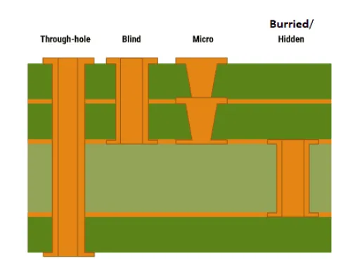
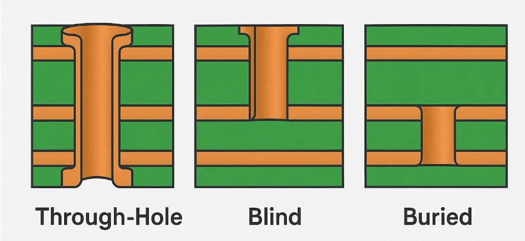
1. Through-Hole Vias
Through-hole vias are the most basic type. They go all the way through the PCB, from the top layer to the bottom layer. These vias are easy to manufacture and are often used for connecting components or mounting holes. However, they take up space on every layer, which can be a drawback in high-density designs where space is limited.
2. Blind Vias
Blind vias connect an outer layer (top or bottom) to one or more inner layers but do not go through the entire board. For instance, a blind via might connect the top layer to the second layer without reaching the bottom. These are useful for saving space on inner layers and are common in high-density interconnect (HDI) designs. However, they are more expensive to fabricate due to the precision required.
3. Buried Vias
Buried vias are hidden within the inner layers of the PCB and do not reach the outer layers. They connect two or more internal layers, leaving the top and bottom surfaces free for components or other routing. Like blind vias, they are ideal for HDI designs but add to manufacturing costs due to their complexity.
4. Microvias
Microvias are very small vias, typically with diameters less than 0.15 mm, used in ultra-compact designs. They are often created using laser drilling and are essential for HDI boards found in devices like smartphones. Microvias can be blind or buried and are stacked or staggered to save even more space. Their small size reduces parasitic effects, making them suitable for high-speed signals above 5 GHz.
5. Stacked and Staggered Vias
Stacked vias are multiple microvias placed directly on top of each other to connect several layers. Staggered vias, on the other hand, are offset from each other to improve reliability and reduce stress during manufacturing. Both are used in advanced HDI designs to maximize space efficiency.
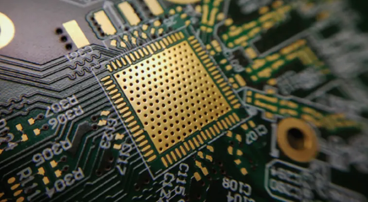
6. Via-in-Pad
In via-in-pad designs, the via is placed directly under a component's pad, often for surface-mount devices like ball grid arrays (BGAs). This saves space and shortens signal paths, improving performance. However, it requires careful manufacturing to avoid solder wicking into the via during assembly.
7. Tented Vias
Tented vias are covered with a layer of solder mask to protect them from external elements or accidental shorting. This is common for vias near the surface that aren't needed for component mounting. Tenting also helps during testing by preventing probes from contacting the via.
8. Thermal Vias
Thermal vias are designed to transfer heat away from components, such as power transistors or processors, to a heat sink or ground plane. They are often arranged in a grid pattern under the component and filled with conductive material to enhance heat dissipation. For instance, a thermal via array might reduce the temperature of a high-power IC by 10-15°C, significantly improving reliability.
How Vias Impact Basic PCB Design
When designing a PCB, vias are more than just holes—they influence the board's performance, cost, and manufacturability. Here are some key considerations for incorporating vias into your design.
Signal Integrity and High-Speed Design
In high-speed circuits, vias can act as bottlenecks if not designed properly. A via introduces impedance discontinuities, which can reflect signals and cause data loss. For designs operating at frequencies above 500 MHz, it's best to minimize the number of vias in critical signal paths. If vias are unavoidable, using smaller diameters (around 0.25 mm) and pairing them with ground vias nearby can reduce noise. Additionally, back-drilling—removing unused portions of through-hole vias—can eliminate stub effects that degrade signal quality.
Power and Ground Distribution
Vias connect power and ground planes across layers, ensuring stable voltage levels. For high-current applications, multiple vias (often 0.3-0.5 mm in diameter) are used in parallel to handle the load and reduce resistance. Placing vias close to power pins of ICs also minimizes voltage drops, which is critical for maintaining performance in digital circuits.
Thermal Management
As mentioned earlier, thermal vias help manage heat in high-power designs. For example, a processor generating 5W of heat might require a grid of 20-30 thermal vias under its package to keep temperatures below 85°C. These vias should connect to a large copper plane to spread heat effectively.
Manufacturing and Cost Considerations
The type and number of vias directly affect the cost of PCB fabrication. Through-hole vias are the cheapest and easiest to produce, while blind, buried, and microvias require advanced techniques like laser drilling or sequential lamination, increasing costs by 20-50%. Balancing performance needs with budget constraints is key. For simpler designs, sticking to through-hole vias can save money without sacrificing functionality.
Best Practices for Using Vias in Multi-Layer PCBs
To make the most of vias in your design, follow these practical tips to optimize performance and avoid common pitfalls.
- Minimize Via Count: Use the fewest vias possible in signal paths to reduce impedance issues and manufacturing costs. Route traces on the same layer when feasible.
- Choose the Right Via Size: Match via diameter to the current or signal requirements. For power connections, use larger vias (0.4-0.6 mm) to handle current; for signals, use smaller vias (0.2-0.3 mm) to minimize capacitance.
- Place Ground Vias Strategically: Add ground vias near signal vias to provide a return path and reduce electromagnetic interference (EMI). A common ratio is one ground via for every two signal vias in high-speed designs.
- Avoid Via Stubs: In high-frequency designs, remove unused via stubs through back-drilling to prevent signal reflections.
- Test and Simulate: Use simulation tools to model via behavior before fabrication. This can help identify potential issues like signal delay or crosstalk early in the design process.
Common Challenges with Vias and How to Overcome Them
While vias are essential, they come with challenges that can impact your PCB's performance if not addressed.
Signal Loss: At high frequencies, vias can cause signal loss due to impedance mismatch. To mitigate this, use shorter vias by routing signals on adjacent layers and avoid unnecessary layer changes.
Manufacturing Defects: Misaligned vias or incomplete plating can lead to open circuits or weak connections. Work with a reliable manufacturer and specify clear design rules, such as minimum via annular ring sizes (typically 0.1 mm around the via) to ensure quality.
Thermal Stress: During soldering, vias can experience thermal stress, especially in via-in-pad designs. Filling vias with epoxy or copper can improve durability and prevent cracking.
Conclusion: Mastering Vias for Better PCB Designs
Vias are the unsung heroes of multi-layer PCBs, enabling complex connections that power today's advanced electronics. From through-hole to microvias, each type serves a unique purpose in balancing space, performance, and cost. By understanding how vias work and following best practices, you can design boards that are efficient, reliable, and ready for high-speed or high-power applications.
Whether you're a beginner learning basic PCB design or an experienced engineer tackling intricate multi-layer layouts, paying attention to vias can make all the difference. With careful planning and the right design choices, these tiny conductive tunnels will ensure your circuits stay connected and perform at their best.