 ALLPCB


If you're new to the world of printed circuit boards (PCBs) and wondering what is heavy copper PCB, or looking to understand the benefits of heavy copper PCB and their applications of heavy copper PCB, you're in the right place. In this beginner's guide, we'll break down the essentials of heavy copper PCBs, why they matter, and how they’re used in various industries. Whether you're just starting with basic PCB knowledge or exploring advanced designs, this article will provide clear, actionable insights to help you understand this powerful technology.
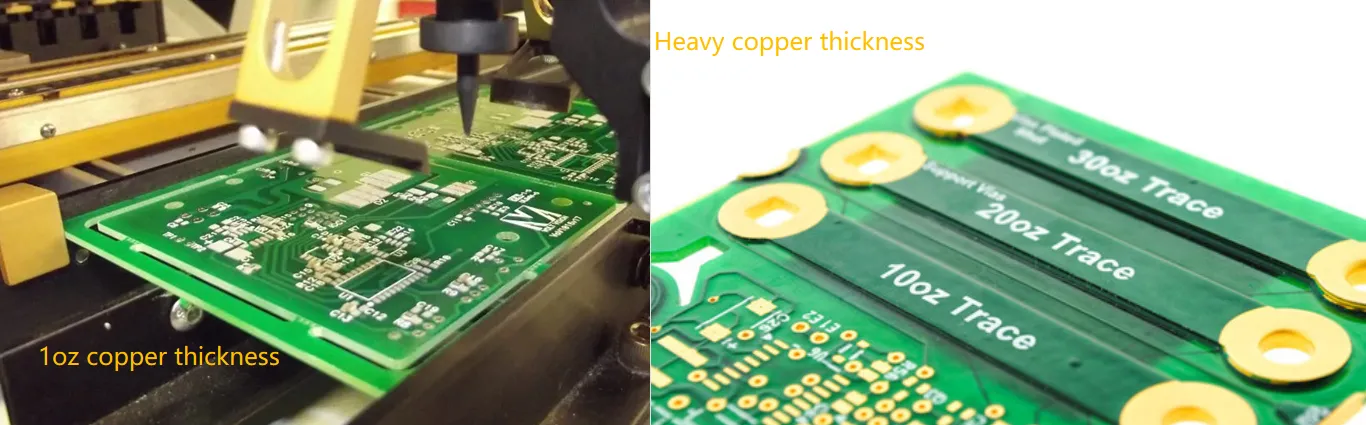
Heavy copper PCBs are a specialized type of circuit board designed with thicker copper layers to handle high current loads and improve heat dissipation. Unlike standard PCBs with copper thicknesses of 1-2 oz/ft2, heavy copper PCBs typically feature copper layers of 3 oz/ft2 or more, making them ideal for demanding applications. In the sections below, we'll dive deeper into their benefits, uses, and why they are a game-changer in modern electronics.
What Is Heavy Copper PCB? A Simple Explanation
Before we explore the advantages and uses, let’s start with the basics: what is heavy copper PCB? A heavy copper PCB is a printed circuit board that has significantly thicker copper layers compared to standard PCBs. While a typical PCB might have copper traces with a thickness of 1 to 2 ounces per square foot (oz/ft2), heavy copper PCBs start at 3 oz/ft2 and can go up to 20 oz/ft2 or more in extreme cases.
The thicker copper allows these boards to carry higher electrical currents without overheating or failing. This makes them a go-to choice for applications where power and durability are critical. The manufacturing process for heavy copper PCBs involves advanced techniques like etching and plating to ensure the copper layers are evenly distributed and robust enough to withstand stress.
Why Choose Heavy Copper PCBs? Key Benefits
Now that you understand what is heavy copper PCB, let’s explore the benefits of heavy copper PCB. These boards offer several advantages that make them stand out in high-power and high-stress environments. Here are the main reasons engineers and designers opt for heavy copper PCBs:
1. Higher Current Carrying Capacity
One of the most significant benefits of heavy copper PCB is their ability to handle high electrical currents. The thicker copper traces reduce electrical resistance, allowing more current to flow through without generating excessive heat. For instance, a standard 1 oz/ft2 copper trace might safely carry around 1-2 amps, while a 5 oz/ft2 heavy copper trace can handle up to 10 amps or more, depending on the design and cooling conditions.
This makes heavy copper PCBs perfect for power electronics where large currents are common, preventing failures due to overheating or trace burnout.
2. Improved Heat Dissipation
Heat management is a critical concern in electronics, especially in high-power applications. Heavy copper PCBs excel at dissipating heat due to the increased thermal conductivity of thicker copper layers. Copper is an excellent conductor of heat, and the added thickness helps spread and release heat more effectively, reducing the risk of hot spots that can damage components.
For example, in a power supply circuit operating at 50 watts, a heavy copper PCB can lower the operating temperature by several degrees compared to a standard board, extending the lifespan of the device.
3. Enhanced Durability and Reliability
Durability is another standout among the benefits of heavy copper PCB. The thicker copper layers make the board more resistant to mechanical stress, vibration, and thermal cycling (repeated heating and cooling). This is especially important in harsh environments where standard PCBs might crack or fail over time.
In applications like automotive electronics, where boards are exposed to constant vibration and temperature changes, heavy copper PCBs ensure long-term reliability, reducing maintenance costs and downtime.
4. Reduced Need for Additional Cooling Systems
Because of their superior heat dissipation, heavy copper PCBs often eliminate the need for external cooling solutions like heat sinks or fans in some designs. This can simplify the overall system design, reduce costs, and save space in compact devices.
For instance, in a high-power LED lighting system, using a heavy copper PCB might allow the design to rely solely on the board for heat management, avoiding the added weight and expense of a separate heat sink.
Applications of Heavy Copper PCB: Where Are They Used?
With a solid grasp of the benefits of heavy copper PCB, let’s look at the applications of heavy copper PCB. These boards are widely used in industries and products that require high power, durability, and heat management. Below are some of the most common areas where heavy copper PCBs shine:
1. Power Electronics and Supplies
Heavy copper PCBs are a staple in power electronics, such as inverters, converters, and power supplies. These devices often deal with high voltages and currents, requiring boards that can handle the load without overheating. For example, a 500-watt power supply unit might use a heavy copper PCB with 6 oz/ft2 thickness to ensure safe and efficient operation.
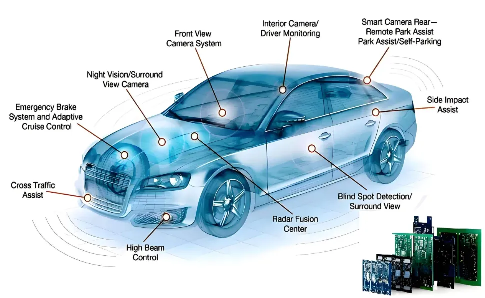
2. Automotive and Electric Vehicles (EVs)
The automotive industry, especially with the rise of electric vehicles, relies heavily on heavy copper PCBs. These boards are used in battery management systems, motor controllers, and charging systems where high current and reliability are non-negotiable. The ability of heavy copper to withstand vibration and thermal stress makes it ideal for the rugged conditions of vehicle electronics.
3. Industrial Equipment and Automation
In industrial settings, heavy copper PCBs are found in equipment like motor drives, welding machines, and robotics. These applications often involve high power and continuous operation, where heat buildup and mechanical stress can degrade standard PCBs. Heavy copper ensures consistent performance even under demanding conditions.
4. Renewable Energy Systems
Solar inverters, wind turbine controllers, and other renewable energy systems benefit from heavy copper PCBs due to their ability to manage high currents and dissipate heat. For instance, a solar inverter converting DC to AC power at 5 kilowatts might use a heavy copper PCB to maintain efficiency and prevent thermal failures in outdoor environments.
5. Military and Aerospace
In military and aerospace applications, reliability is critical. Heavy copper PCBs are used in radar systems, communication devices, and power distribution units where failure is not an option. Their robustness against extreme temperatures and mechanical stress ensures performance in challenging conditions.
Basic PCB Knowledge: Understanding the Foundation
For those just starting with basic PCB knowledge, it’s helpful to understand how heavy copper PCBs fit into the broader world of circuit board design. A PCB, or printed circuit board, is the foundation of most electronic devices. It provides a platform to mount components like resistors, capacitors, and microchips, while copper traces connect these components to form a working circuit.
Standard PCBs use thin copper layers to keep costs low and suit low-power applications like consumer gadgets. However, as power demands increase, so does the need for thicker copper, leading to the development of heavy copper PCBs. Here are a few key points of basic PCB knowledge to keep in mind:
- Copper Thickness: Measured in ounces per square foot (oz/ft2), copper thickness determines how much current a trace can carry. Standard PCBs are typically 1-2 oz/ft2, while heavy copper starts at 3 oz/ft2.
- Trace Width: Wider traces can carry more current, but heavy copper allows for higher current in narrower traces, saving space on the board.
- Layers: PCBs can have multiple layers of copper (e.g., 2-layer, 4-layer). Heavy copper can be applied to any layer for power distribution or grounding.
Understanding these basics helps highlight why heavy copper PCBs are a specialized solution for specific challenges in electronics design.
Challenges and Considerations with Heavy Copper PCBs
While the benefits of heavy copper PCB are impressive, it’s worth noting a few challenges and considerations. These boards are more expensive to manufacture due to the increased material costs and specialized processes involved. The thicker copper also requires precise etching to avoid undercutting or uneven traces, which can impact signal integrity if not done correctly.
Additionally, heavy copper PCBs are heavier and may not be suitable for applications where weight is a critical factor, such as portable devices. Designers must balance the advantages of heavy copper with the specific needs of their project to ensure the best outcome.
How Heavy Copper PCBs Are Manufactured
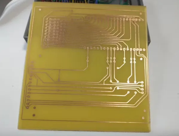
For those curious about the behind-the-scenes process, manufacturing heavy copper PCBs involves several unique steps. It starts with laminating a substrate material, like FR-4, with thick copper foil. The copper is then etched to create the desired circuit pattern, often requiring more powerful chemicals or longer etching times due to the thickness.
In some cases, additional copper is plated onto the traces to achieve the desired thickness, a process known as electroplating. Finally, the board undergoes rigorous testing to ensure it meets current-carrying and thermal performance standards. This meticulous process ensures that heavy copper PCBs deliver the reliability and performance needed for high-power applications.
Why Heavy Copper PCBs Matter for Your Projects
Whether you're an engineer, hobbyist, or business owner exploring PCB options, understanding the benefits of heavy copper PCB and their applications of heavy copper PCB can make a big difference in your projects. These boards offer unmatched performance in high-current, high-heat scenarios, ensuring your designs are reliable and efficient.
From power supplies to electric vehicles, heavy copper PCBs play a vital role in modern technology. By choosing the right type of PCB for your needs, you can avoid common issues like overheating or premature failure, ultimately saving time and resources.
Conclusion: Unlocking the Power of Heavy Copper PCBs
In this beginner's guide, we've covered the essentials of what is heavy copper PCB, the key benefits of heavy copper PCB, and the diverse applications of heavy copper PCB. We've also touched on basic PCB knowledge to provide a foundation for understanding why heavy copper is a specialized yet powerful solution in electronics design.
Heavy copper PCBs stand out for their ability to handle high currents, dissipate heat effectively, and offer long-lasting durability. They are indispensable in industries like automotive, renewable energy, and industrial automation, where performance and reliability are critical. As you dive deeper into PCB design, keep heavy copper in mind for projects that demand more power and resilience.
With this knowledge, you're better equipped to make informed decisions about incorporating heavy copper PCBs into your next project. Their unique advantages can help you achieve superior results in challenging applications, paving the way for innovative and dependable electronic solutions.


