 ALLPCB


In the fast-evolving world of telecommunications, base station printed circuit boards (PCBs) play a critical role in ensuring seamless connectivity and high-speed data transfer. As we look toward the future, what are the key trends and innovations shaping PCB technology for telecommunication base stations? This blog dives deep into PCB technology trends, telecommunications PCB innovation, and cutting-edge developments like advanced PCB materials, flexible PCBs, and 3D PCBs. Whether you're an engineer or a tech enthusiast, you'll find actionable insights into how these advancements are driving the industry forward in 2025 and beyond.
Why Telecommunication Base Station PCBs Matter
Telecommunication base stations are the backbone of modern wireless networks, supporting everything from 5G connectivity to IoT applications. The PCBs within these stations handle high-frequency signals, power distribution, and data processing under demanding conditions. As network demands grow, so does the need for innovative PCB solutions that can manage higher speeds, reduce signal loss, and fit into increasingly compact designs.
With global 5G rollout accelerating—expected to cover over 60% of the world's population by 2030, according to industry forecasts—base station PCBs must evolve to meet these challenges. Let’s explore the trends and innovations paving the way for the future.
Key PCB Technology Trends Shaping Telecommunications
The PCB industry is undergoing rapid transformation to keep up with the demands of telecommunications. Below are the most impactful PCB technology trends for base stations in 2025 and beyond.
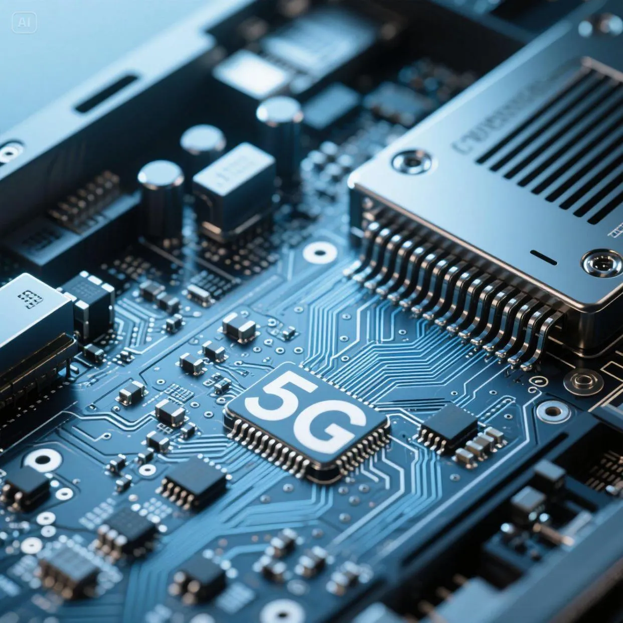
1. High-Frequency Materials for 5G and Beyond
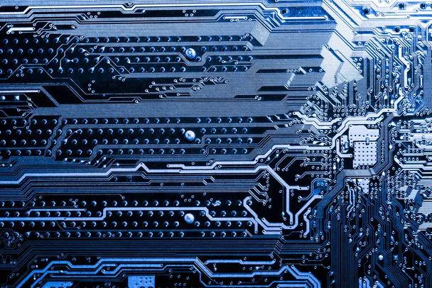
5G networks operate at higher frequencies, often in the range of 24 GHz to 100 GHz, compared to 4G's lower bands. This shift requires PCBs to use advanced PCB materials with low dielectric constants and minimal signal loss. Materials like PTFE (polytetrafluoroethylene) and high-speed laminates are becoming standard for base station PCBs, as they maintain signal integrity at these elevated frequencies.
For example, a typical high-frequency PCB material might have a dielectric constant (Dk) of around 2.2 and a dissipation factor (Df) of 0.0009, ensuring minimal signal distortion over long distances. These materials also help manage thermal dissipation, a critical factor in base stations that operate continuously under high loads.
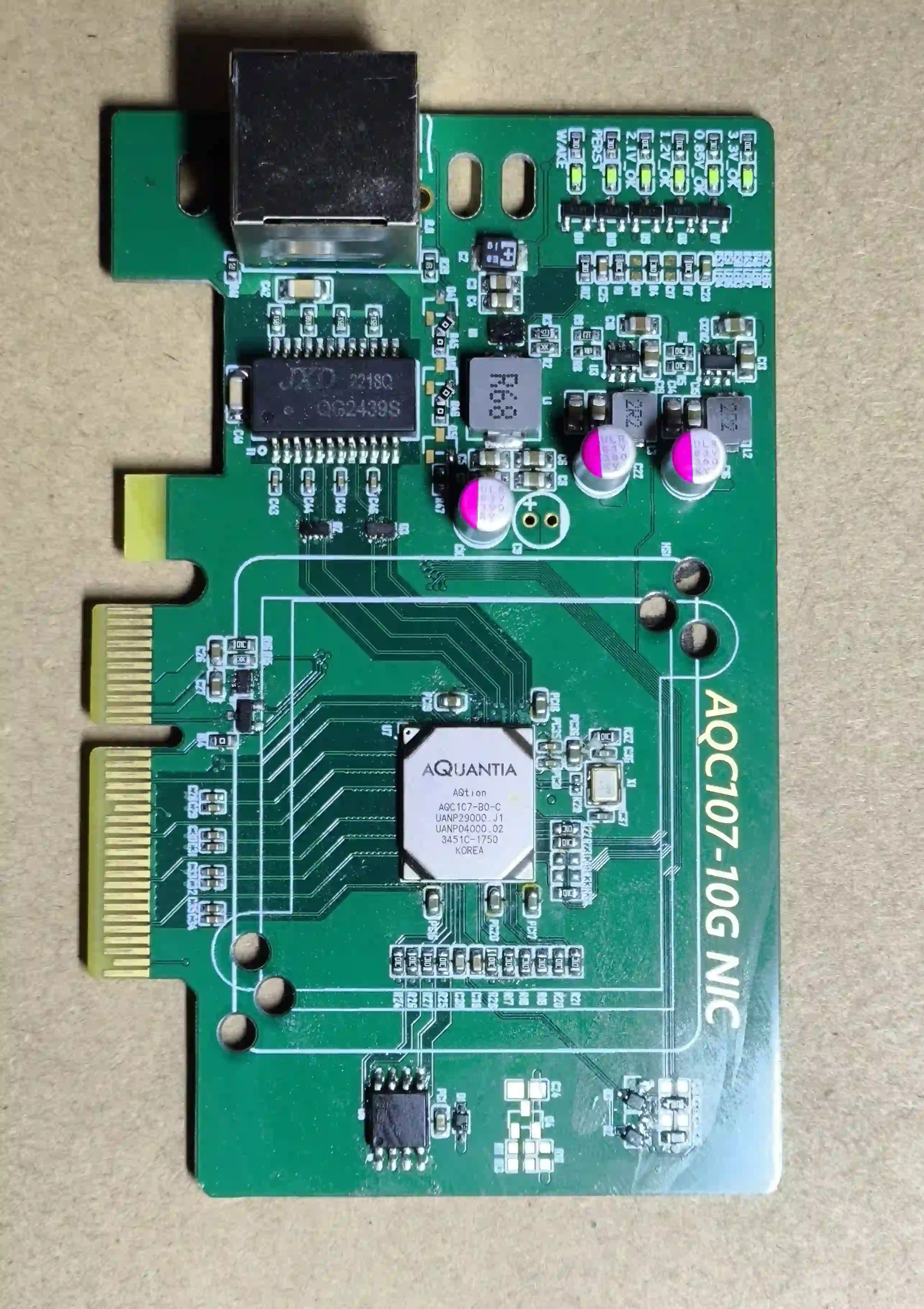
2. Miniaturization and High-Density Interconnects (HDI)
As base stations become more compact to fit urban environments, PCB designs must shrink without sacrificing performance. High-density interconnect (HDI) technology allows for more components to be packed into smaller spaces through microvias and finer trace widths, often as narrow as 50 micrometers. This trend is essential for base stations that need to support multiple frequency bands and advanced antenna systems in limited space.
Miniaturization also reduces power consumption and improves signal routing efficiency, directly impacting the overall performance of telecommunication networks.
3. Thermal Management Innovations
Base stations generate significant heat due to continuous operation and high power levels, often exceeding 100 watts per module. Effective thermal management in PCBs is crucial to prevent overheating and ensure reliability. Innovations like metal-core PCBs and embedded heat sinks are gaining traction. These designs use materials with high thermal conductivity, such as aluminum or copper, to dissipate heat efficiently.
Additionally, advanced simulation tools now allow engineers to predict thermal behavior during the design phase, ensuring optimal performance under real-world conditions. For instance, a well-designed thermal PCB can maintain operating temperatures below 85°C, even in harsh environments.
Telecommunications PCB Innovation: Pushing the Boundaries
Beyond general trends, specific telecommunications PCB innovations are redefining how base stations operate. These breakthroughs address the unique challenges of high-speed data, durability, and scalability.
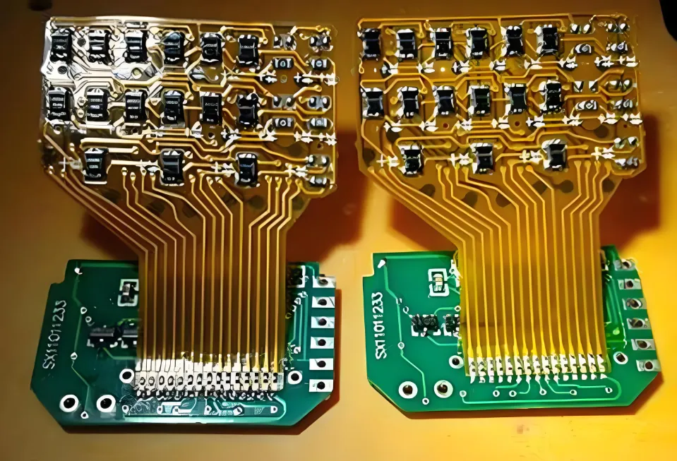
1. Adoption of Flexible PCBs for Compact Designs
Flexible PCBs are becoming a game-changer for telecommunication base stations, especially in applications where space and weight are critical. Unlike rigid boards, flexible PCBs can bend and conform to irregular shapes, allowing for more efficient use of space within compact base station enclosures.
For instance, flexible PCBs are often used in antenna modules, where they can wrap around components to save space while maintaining signal integrity. They are made from polyimide materials that withstand bending without cracking, ensuring long-term reliability even in dynamic environments. This innovation is particularly valuable for small cell base stations deployed in dense urban areas.
2. Emergence of 3D PCBs for Enhanced Functionality
Another exciting development is the use of 3D PCBs, which stack multiple layers of circuitry in a three-dimensional structure. This approach maximizes space efficiency and reduces the footprint of base station hardware. 3D PCBs are particularly useful for integrating complex systems like RF (radio frequency) modules and power amplifiers into a single, compact unit.
By using additive manufacturing techniques, 3D PCBs can also incorporate unique geometries that improve signal routing and reduce interference. For example, a 3D PCB might reduce signal path length by 20%, improving latency in high-speed 5G networks. This technology is still evolving, but its potential for base stations is immense.
3. Advanced Surface Finishes for Durability
Base stations often operate in harsh outdoor environments, exposed to moisture, dust, and temperature fluctuations. To combat these challenges, PCB manufacturers are adopting advanced surface finishes like immersion silver and ENIG (Electroless Nickel Immersion Gold). These finishes provide superior corrosion resistance and ensure reliable solder joints over time.
For instance, ENIG offers a flat surface for fine-pitch components and can withstand multiple reflow cycles without degrading, making it ideal for the rigorous demands of telecommunication hardware.
The Role of Advanced PCB Materials in Future Base Stations
As mentioned earlier, advanced PCB materials are central to meeting the performance demands of modern telecommunications. Let’s dive deeper into how these materials are shaping the future of base station PCBs.
1. Low-Loss Materials for High-Speed Signals
High-speed data transmission in 5G and future 6G networks requires materials that minimize signal loss. Low-loss laminates, often with a dissipation factor below 0.002, are critical for maintaining signal strength over long traces. These materials also support higher layer counts, enabling complex multi-layer PCB designs without compromising performance.
For example, a base station PCB designed for millimeter-wave frequencies might use a specialized laminate to achieve signal speeds exceeding 10 Gbps with minimal attenuation.
2. Eco-Friendly and Sustainable Materials
Sustainability is becoming a priority in PCB manufacturing. With electronic waste growing globally, manufacturers are exploring halogen-free materials and recyclable substrates to reduce environmental impact. These eco-friendly materials maintain performance standards while aligning with stricter regulations on hazardous substances.
In telecommunications, adopting sustainable materials for base station PCBs not only supports green initiatives but also enhances brand reputation in an environmentally conscious market.
Challenges and Solutions in Base Station PCB Design
While innovations are driving progress, challenges remain in designing PCBs for telecommunication base stations. Below are some common hurdles and how the industry is addressing them.
1. Signal Integrity at High Frequencies
At high frequencies, signal integrity becomes a major concern due to crosstalk and impedance mismatches. Designers are using controlled impedance techniques, ensuring trace impedance stays within tight tolerances (e.g., ±5% of 50 ohms for RF lines). Advanced simulation software also helps identify potential issues before manufacturing, saving time and costs.
2. Cost vs. Performance Balance
Advanced materials and technologies often come with higher costs, which can be a barrier for large-scale deployment. To address this, manufacturers are optimizing designs to use hybrid materials—combining high-performance substrates only where needed and cost-effective options elsewhere. This approach ensures performance without breaking the budget.
How These Trends Benefit Engineers and Manufacturers
For engineers working on telecommunication base stations, staying ahead of PCB technology trends offers several advantages. First, adopting innovations like flexible PCBs and 3D PCBs allows for more creative and efficient designs, meeting the needs of next-generation networks. Second, using advanced PCB materials ensures reliability and performance, reducing maintenance costs over time.
For manufacturers, these trends open up new opportunities to differentiate their offerings. By investing in cutting-edge technologies and sustainable practices, they can cater to the growing demand for high-performance base station hardware while aligning with global standards.
Looking Ahead: The Future of Base Station PCBs
The future of telecommunication base station PCBs is bright, with continuous advancements in materials, design techniques, and manufacturing processes. As 5G matures and 6G emerges on the horizon, the need for innovative solutions will only grow. Trends like telecommunications PCB innovation, flexible PCBs, and 3D PCBs will play a pivotal role in shaping how we connect in the coming decades.
By embracing these technologies today, engineers and manufacturers can build the foundation for faster, more reliable, and more sustainable telecommunication networks tomorrow. Whether it’s through adopting new materials or exploring novel design approaches, the possibilities are endless.

Conclusion
Telecommunication base station PCBs are at the heart of modern connectivity, and their evolution is critical to meeting the demands of 5G and beyond. From advanced PCB materials that support high-frequency signals to flexible PCBs and 3D PCBs that enable compact designs, the latest PCB technology trends are transforming the industry. By understanding and leveraging these innovations, engineers and manufacturers can stay ahead in a competitive and rapidly changing field.
At ALLPCB, we’re committed to supporting the telecommunication industry with cutting-edge PCB solutions tailored to your needs. Explore how these trends can enhance your next base station project and keep you at the forefront of connectivity.


