 ALLPCB


If you're looking to optimize your PCB designs with stacked vias, you're in the right place. Stacked vias are a critical element in high-density interconnect (HDI) boards, allowing for efficient layer transitions in compact designs. But how do you ensure they're implemented correctly? This guide dives into stacked via design rules, stacked via clearance, stacked via aspect ratio, stacked via drill size, and stacked via IPC standards to help you master their use. Let’s explore the best practices to ensure reliability, performance, and manufacturability in your PCB projects.
Recommended Reading: The Ultimate Guide to Stacked Vias in High-Density PCBs
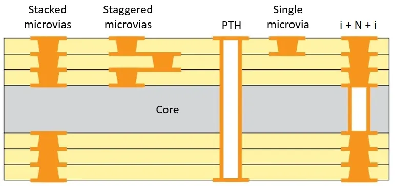
What Are Stacked Vias and Why Do They Matter?
Stacked vias are vertical interconnects placed directly on top of each other to connect multiple layers in a printed circuit board (PCB). Unlike staggered vias, which are offset, stacked vias save space, making them ideal for HDI designs where real estate is limited. They are commonly used in complex electronics like smartphones, tablets, and advanced medical devices.
The importance of stacked vias lies in their ability to support high-speed signals and dense layouts. However, improper design can lead to issues like signal degradation, manufacturing defects, or structural weaknesses. That's why understanding the rules and best practices for stacked via design is essential for any PCB engineer aiming for reliable and efficient boards.
Key Stacked Via Design Rules for Success
Designing stacked vias requires adherence to specific guidelines to ensure functionality and manufacturability. Below are the core stacked via design rules to follow:
- Alignment Precision: Stacked vias must be perfectly aligned vertically to avoid connectivity issues. Misalignment can cause incomplete connections or stress points during manufacturing. Use design software with precise grid and alignment tools to maintain accuracy.
- Layer Limitations: Limit the number of layers a stacked via spans. Typically, stacking across 2-3 layers is manageable, but exceeding this can increase the risk of structural failure due to thermal expansion or drilling inaccuracies.
- Via Filling: Consider filling stacked vias with conductive material to enhance reliability and reduce the risk of voids during plating. This is especially important for high-current applications.
Following these rules ensures that your stacked vias perform as intended without compromising the board's integrity. Always consult your fabrication partner for specific capabilities, as some may have stricter constraints based on their equipment and processes.
Understanding Stacked Via Clearance for Signal Integrity
Stacked via clearance refers to the minimum spacing between vias and surrounding traces or other vias. Proper clearance is critical to prevent electrical interference, crosstalk, and short circuits, especially in high-speed designs.
For example, in a design operating at 5 GHz, inadequate clearance between stacked vias and adjacent signal traces can lead to crosstalk, degrading signal quality. A general rule of thumb is to maintain a clearance of at least 3 times the via diameter between stacked vias and nearby traces. However, for high-frequency signals, you may need to increase this to 5 times the diameter or more, depending on the dielectric material and stackup.
Additionally, ensure that stacked vias are spaced adequately from each other. A minimum spacing of 8-10 mils (0.2-0.25 mm) between via centers is often recommended for standard designs, though this can vary based on board density and manufacturing tolerances.
Stacked Via Aspect Ratio: Balancing Design and Manufacturability
The stacked via aspect ratio is the ratio of the via's depth to its diameter. This parameter is crucial because it impacts both the ease of manufacturing and the via's reliability. A high aspect ratio (e.g., 10:1) means a deep, narrow via, which can be challenging to drill and plate uniformly. A low aspect ratio (e.g., 3:1) is easier to fabricate but may require a larger diameter, taking up more board space.
For stacked vias, aim for an aspect ratio between 3:1 and 5:1 to balance manufacturability and design constraints. For instance, if your via depth spans 30 mils (0.76 mm) across layers, the drill diameter should ideally be between 6-10 mils (0.15-0.25 mm). Exceeding a 5:1 ratio often leads to plating issues, such as uneven copper deposition, which can cause open circuits or weak connections.
Always check with your manufacturer for their maximum supported aspect ratio, as advanced HDI processes may allow ratios up to 8:1, while standard processes might be limited to 4:1.
Recommended Reading: Via Aspect Ratio: The Unsung Hero of PCB Reliability
Choosing the Right Stacked Via Drill Size
Selecting the appropriate stacked via drill size is a critical step in the design process. The drill size determines the via’s diameter and directly affects the aspect ratio, current-carrying capacity, and manufacturing feasibility.
For microvias, which are often used in stacked configurations, drill sizes typically range from 3 to 6 mils (0.075 to 0.15 mm). Standard vias might use drill sizes of 8 to 12 mils (0.2 to 0.3 mm). Smaller drill sizes are preferred in HDI designs to save space, but they come with challenges like higher drilling precision requirements and increased costs.
Keep in mind that the finished via diameter will be slightly larger than the drill size due to plating. For instance, a 6-mil drill might result in a finished via diameter of 7-8 mils after copper plating. Also, ensure the drill size supports the current requirements of your design. A via carrying 1 amp of current might need a minimum diameter of 10 mils to prevent overheating, based on standard current density calculations.
Adhering to Stacked Via IPC Standards
The stacked via IPC standards provide guidelines to ensure quality and reliability in PCB manufacturing. These standards, developed by the Institute of Printed Circuits, cover various aspects of via design, including dimensions, spacing, and manufacturing processes.
Key IPC standards relevant to stacked vias include:
- IPC-2221: This standard outlines generic design principles for PCBs, including via spacing and clearance. It recommends minimum clearances based on voltage levels to prevent electrical breakdown. For instance, at 100V, a clearance of at least 0.25 mm is advised between conductive elements.
- IPC-6012: Focuses on the qualification and performance of rigid PCBs. It specifies requirements for via plating thickness and quality, ensuring stacked vias can withstand thermal and mechanical stress. A minimum plating thickness of 20-25 microns is often required for reliability.
- IPC-4761: Covers via protection and filling methods. For stacked vias, it suggests conductive filling or capping to prevent voids and enhance structural integrity.
Compliance with these standards not only improves the reliability of your design but also ensures compatibility with most fabrication houses. Non-compliance can lead to manufacturing delays or boards that fail during testing or operation.
Best Practices for Stacked Via Design
Beyond following specific rules and standards, adopting best practices can elevate the quality of your stacked via designs. Here are actionable tips to implement:
- Use Simulation Tools: Before finalizing your design, use simulation software to analyze signal integrity and thermal performance. This helps identify potential issues with stacked vias, such as impedance mismatches at high frequencies (e.g., above 1 GHz) or excessive heat buildup in vias carrying 2 amps or more.
- Optimize Stackup Design: Plan your PCB stackup to minimize the number of layers a stacked via must span. For example, placing high-speed signals on adjacent layers reduces via length and improves performance.
- Collaborate with Manufacturers Early: Engage with your fabrication partner during the design phase to understand their capabilities for drilling, plating, and via filling. Some manufacturers may struggle with aspect ratios above 4:1 or drill sizes below 5 mils.
- Test for Reliability: After fabrication, conduct thorough testing, including thermal cycling and electrical continuity tests, to ensure stacked vias perform under real-world conditions. A failure rate of even 0.1% can be catastrophic in critical applications.
Common Challenges with Stacked Vias and How to Avoid Them
While stacked vias offer significant benefits, they come with challenges that can impact your design if not addressed. Here are some common issues and solutions:
- Drilling Misalignment: Misaligned drills can create disconnected or weak stacked vias. Use advanced design tools with automated alignment checks and work with manufacturers who use laser drilling for precision.
- Thermal Stress: Stacked vias spanning multiple layers are prone to thermal expansion stress, which can cause cracking. Limit via height and use materials with matching coefficients of thermal expansion (CTE) for the via and board substrate.
- Signal Loss: High-speed signals passing through stacked vias can experience loss due to impedance discontinuities. Minimize via length and use back-drilling to remove unused via stubs, reducing signal reflection.
Conclusion: Elevate Your PCB Design with Stacked Vias
Mastering stacked via design rules, stacked via clearance, stacked via aspect ratio, stacked via drill size, and stacked via IPC standards is key to creating high-performance, reliable PCBs. By following the guidelines and best practices outlined in this guide, you can avoid common pitfalls and ensure your designs meet both functional and manufacturing requirements.
Stacked vias are a powerful tool for HDI designs, enabling compact layouts without sacrificing connectivity. Whether you're working on a high-speed communication device or a compact consumer gadget, proper via design can make all the difference. Take the time to plan, simulate, and collaborate with your fabrication team to achieve the best results.
With these insights, you're well-equipped to tackle stacked via design challenges and elevate your PCB projects to new levels of efficiency and reliability. Keep these rules and practices in mind for every design, and you'll see consistent improvements in performance and manufacturability.


