 ALLPCB


If you're diving into rigid-flex PCB design, one of the most critical aspects to master is setting up Design Rule Checks (DRC) for bending and folding areas. How do you ensure your design withstands the mechanical stress of repeated flexing while maintaining electrical performance? The answer lies in tailoring DRC specifically for the unique challenges of rigid-flex boards, focusing on bend area design rules, material constraints, and manufacturing tolerances. In this comprehensive guide, we'll walk you through the essentials of rigid-flex PCB DRC, flexible design rules, and best practices for bend area optimization to help you create reliable, high-performance designs.
What is Rigid-Flex PCB Design and Why DRC Matters
Rigid-flex PCBs combine the benefits of rigid and flexible circuits into a single board, allowing for compact, lightweight designs that can bend or fold to fit into tight spaces. These boards are widely used in industries like aerospace, medical devices, and consumer electronics where space constraints and durability are critical. However, the combination of rigid and flexible sections introduces unique design challenges, especially in areas that will be bent or folded during use.
Design Rule Checks (DRC) are a set of predefined rules in PCB design software that ensure your layout meets manufacturing and performance standards. For rigid-flex designs, DRC must account for both electrical requirements (like trace spacing and via placement) and mechanical constraints (like bend radius and material stress). Failing to tailor DRC for bending and folding can lead to issues like cracked traces, delamination, or complete board failure. By customizing DRC for flexible areas, you can catch potential problems early and ensure a robust design.
Key Challenges in Rigid-Flex PCB Design for Bending and Folding
Designing a rigid-flex PCB that can handle bending and folding requires addressing several challenges. Unlike fully rigid boards, the flexible sections are subject to mechanical stress that can impact both structural integrity and electrical performance. Here are the primary challenges to consider:
- Mechanical Stress: Repeated bending can cause fatigue in materials, leading to cracks in copper traces or dielectric layers.
- Bend Radius Limitations: Each flexible material has a minimum bend radius, and violating this can result in permanent damage.
- Transition Zones: The areas where rigid and flexible sections meet are prone to stress concentration, requiring careful design to prevent failure.
- Trace Routing: Traces in flexible areas must be designed to minimize stress, often requiring wider spacing or specific patterns.
DRC helps address these challenges by enforcing rules that prevent design errors, such as placing components too close to bend areas or using inappropriate materials. Let’s dive into how to set up DRC for these unique requirements.
Setting Up DRC for Rigid-Flex PCB Design
Customizing DRC for rigid-flex designs involves defining rules that cater to both the rigid and flexible sections of the board. Most PCB design tools allow you to create separate rule sets for different areas of the board, which is essential for rigid-flex layouts. Below are the key DRC considerations for bending and folding.
1. Define Bend Areas and Zones
The first step in tailoring DRC is to clearly define the bend areas in your design software. These are the regions of the board that will be flexed or folded during use. By marking these zones, you can apply specific rules to ensure they meet mechanical and electrical requirements. For example, you might set a rule that prevents components from being placed within 2 mm of a bend area to avoid stress on solder joints.
2. Enforce Minimum Bend Radius Rules
Every flexible material has a minimum bend radius, which is the smallest curve the material can handle without damage. For instance, a typical polyimide-based flex material might have a minimum bend radius of 6 times the thickness of the flex layer (e.g., for a 0.1 mm thick layer, the bend radius should be at least 0.6 mm). DRC should include a check to ensure that the design adheres to this limit. Violating the bend radius can cause cracking or delamination, leading to board failure.
3. Control Trace Routing in Flexible Areas
Traces in bend areas must be routed to minimize mechanical stress. DRC rules for flexible design should include:
- Wider Trace Spacing: Increase spacing between traces in flex areas to reduce the risk of short circuits during bending. A common rule is to maintain at least 0.2 mm spacing.
- Curved Traces: Avoid sharp corners in traces, as they can act as stress points. Use curved or teardrop-shaped transitions instead.
- Trace Orientation: Route traces perpendicular to the bend line to minimize strain. For a bend radius of 1 mm, ensure traces are at least 0.1 mm wide to maintain integrity.
Setting up DRC to flag violations of these rules ensures that your traces can withstand repeated flexing without breaking.
4. Restrict Via Placement Near Bend Areas
Vias are rigid structures that can crack or fail under mechanical stress. DRC should prevent vias from being placed within a specified distance (e.g., 1 mm) of bend areas. If vias are unavoidable, consider using teardrop-shaped pads to reduce stress concentration. Additionally, ensure that vias in flex areas are not plated through if possible, as this can increase stiffness and risk of failure.
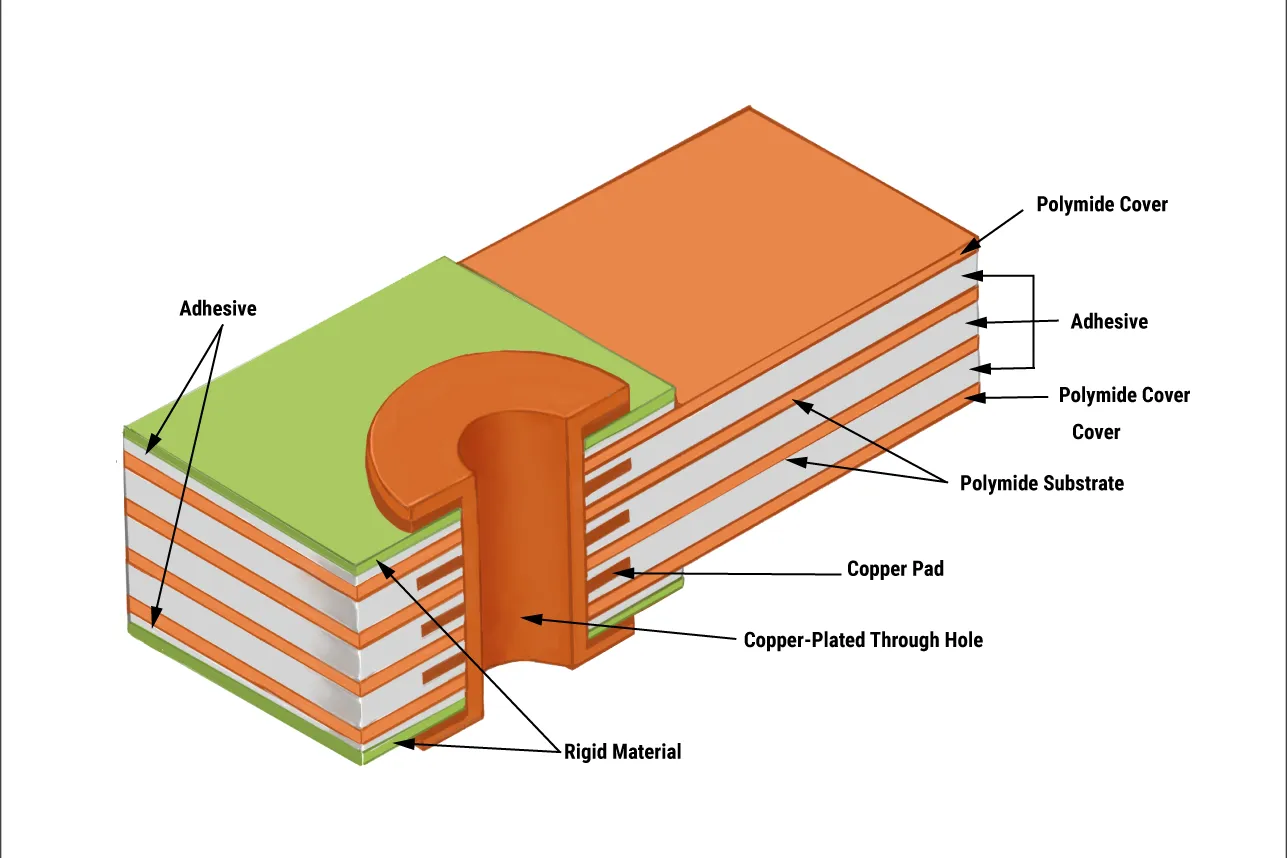
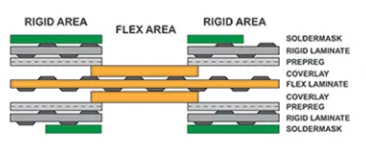
5. Material and Stackup Constraints
The choice of materials and stackup design plays a significant role in the flexibility and durability of a rigid-flex PCB. DRC can enforce rules related to material selection, such as ensuring that only adhesive-less polyimide materials are used in flex areas to reduce thickness and improve flexibility. For a 4-layer rigid-flex design, a common stackup might include a 0.1 mm flex core with 0.035 mm copper layers, balanced to minimize stress. DRC should flag any deviations from the recommended stackup to prevent manufacturing issues.
Flexible Design Rules for Bend Area Optimization
Beyond DRC setup, there are several flexible design rules specific to bend areas that can enhance the reliability of your rigid-flex PCB. These rules focus on minimizing stress and ensuring manufacturability.
1. Use Stiffeners in Transition Zones
Transition zones between rigid and flexible areas are particularly vulnerable to stress. Adding stiffeners—thin layers of rigid material like FR4—can reinforce these areas and prevent cracking. DRC can include a rule to ensure stiffeners are placed at least 0.5 mm away from the actual bend line to avoid restricting flexibility.
2. Optimize Coverlay and Adhesive Placement
Coverlay, the protective layer over flexible circuits, should extend slightly beyond the bend area to protect traces from environmental damage. DRC rules can enforce a minimum overlap of 0.3 mm for coverlay in flex zones. Similarly, avoid using adhesives in high-stress bend areas, as they can increase stiffness and lead to delamination.
3. Account for Dynamic vs. Static Flexing
Not all rigid-flex designs are bent the same way. Dynamic flexing (repeated bending) requires stricter design rules than static flexing (bent once during assembly). For dynamic flexing, DRC might enforce a larger bend radius (e.g., 10 times the flex thickness) and limit the number of copper layers in the flex area to reduce stiffness. For static flexing, a smaller bend radius (e.g., 6 times the thickness) may be acceptable.
Best Practices for Rigid-Flex PCB DRC Implementation
To ensure your DRC setup is effective for bending and folding, follow these best practices:
- Collaborate with Manufacturers: Work closely with your PCB fabricator to understand their specific capabilities and constraints. For instance, some manufacturers may require a minimum drill-to-copper clearance of 0.25 mm in flex areas.
- Test DRC Iteratively: Run DRC checks at multiple stages of the design process to catch issues early. Adjust rules as needed based on feedback from simulations or prototypes.
- Simulate Mechanical Stress: Use simulation tools to model bending and folding behavior. This can help validate DRC rules, such as ensuring a bend radius of 0.8 mm does not exceed the material’s stress limit of 150 MPa.
- Document Rules: Maintain a detailed record of your DRC settings for each project. This ensures consistency and makes it easier to update rules for future designs.
Common DRC Mistakes to Avoid in Rigid-Flex Design
Even with a solid DRC setup, it’s easy to overlook critical details in rigid-flex design. Here are some common mistakes to watch out for:
- Ignoring Bend Radius Limits: Designing a bend radius smaller than the material’s specification can lead to immediate or long-term failure.
- Placing Components in Bend Areas: Components, even small ones, can cause stress points and should be restricted to rigid sections.
- Overlooking Transition Zone Stress: Failing to reinforce or properly design transition areas can result in cracks or delamination.
- Inconsistent Stackup: Using an unbalanced stackup can create uneven stress distribution, leading to board warping.
By incorporating checks for these issues into your DRC, you can prevent costly redesigns and ensure a reliable product.
Conclusion: Mastering Rigid-Flex PCB DRC for Bending and Folding
Rigid-flex PCB design offers incredible potential for creating compact, durable electronics, but it comes with unique challenges in bending and folding areas. Tailoring DRC for these designs is essential to ensure both mechanical reliability and electrical performance. By defining bend areas, enforcing minimum bend radius rules, controlling trace routing, and adhering to flexible design rules, you can create robust rigid-flex boards that meet the demands of modern applications.
Whether you're designing for dynamic flexing in a wearable device or static folding in a compact gadget, a well-configured DRC setup is your first line of defense against design errors. Take the time to customize your rules, collaborate with manufacturers, and simulate stress conditions to achieve a design that’s built to last. With these strategies, you’ll be well on your way to mastering rigid-flex PCB DRC for bending and folding.


