ALLPCB


If you're looking for an RF PCB prototyping service that delivers quick results, or need insights on RF PCB quick turn prototype options, assembly, costs, and testing, you've come to the right place. At ALLPCB, we understand the importance of speed and precision in bringing your RF designs to life. In this comprehensive guide, we'll walk you through the best techniques for fast and efficient RF PCB prototyping, covering everything from design tips to cost considerations and testing methods. Whether you're an engineer validating a new concept or a startup iterating on hardware, this blog will help you streamline your process and achieve reliable results.
What is RF PCB Prototyping and Why Does It Matter?
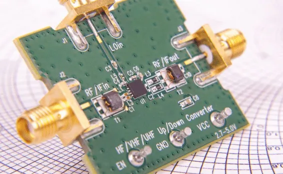
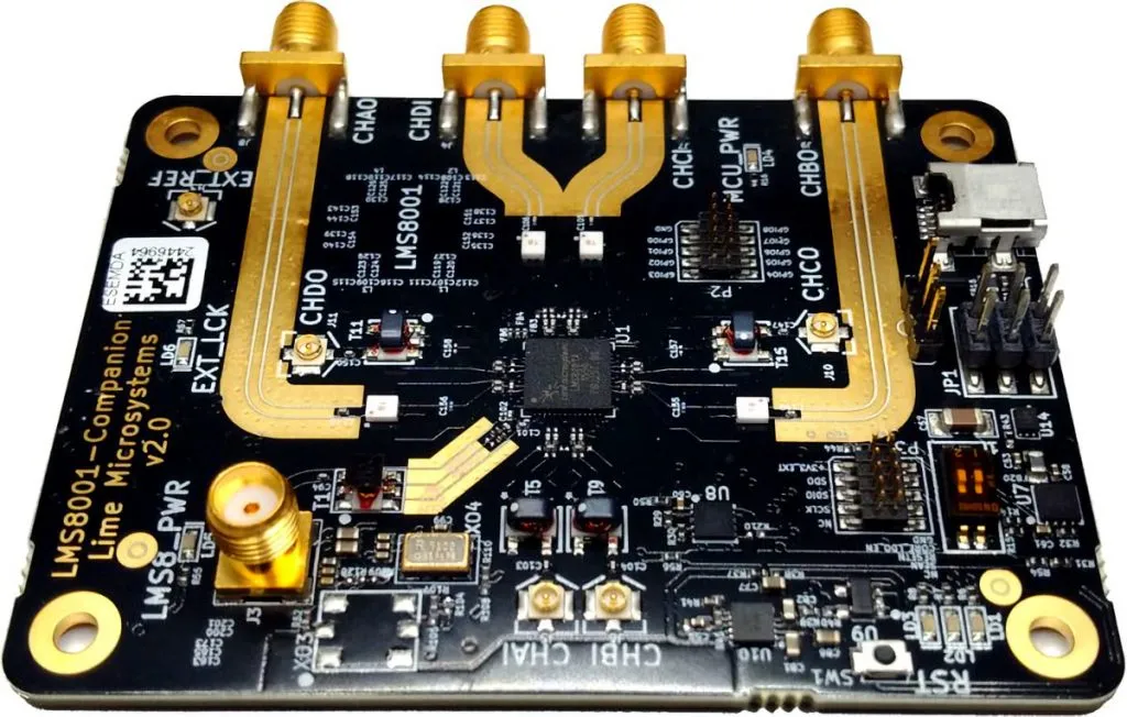
RF PCB prototyping involves creating early versions of printed circuit boards designed specifically for radio frequency applications. These boards handle high-frequency signals, often in the range of 100 MHz to several GHz, and are used in industries like telecommunications, aerospace, automotive radar, and IoT devices. Unlike standard PCBs, RF boards require special attention to signal integrity, impedance control, and material selection due to the sensitivity of high-frequency signals.
The prototyping phase is critical because it allows engineers to test and validate their designs before moving to full-scale production. A well-executed prototype can save time, reduce costs, and prevent costly redesigns by identifying issues early. With an RF PCB quick turn prototype, you can accelerate your development cycle and get products to market faster.
Key Challenges in RF PCB Prototyping
Designing and prototyping RF PCBs comes with unique challenges due to the nature of high-frequency signals. Here are some of the most common hurdles engineers face:
- Signal Integrity: At high frequencies, even small design flaws can cause signal loss, crosstalk, or interference. Maintaining consistent impedance, often around 50 ohms for many RF applications, is crucial.
- Material Selection: Standard FR-4 materials may not perform well at higher frequencies due to dielectric losses. Specialized materials like Rogers or Teflon-based laminates are often required.
- Layout Precision: The placement of components, trace lengths, and grounding techniques directly impact performance. For example, mismatched trace lengths in differential pairs can introduce phase errors.
- Testing Complexity: Validating an RF design requires specialized equipment like vector network analyzers (VNAs) to measure parameters such as S-parameters and return loss.
Overcoming these challenges requires a combination of careful design practices and access to reliable prototyping services. Let’s explore how to achieve fast and efficient results with an RF PCB prototyping service.
Fast and Efficient Techniques for RF PCB Prototyping
1. Optimize Your Design for Prototyping
Before sending your design for fabrication, take steps to ensure it’s optimized for RF performance. Start by defining your frequency range and impedance requirements. For instance, if you’re working on a 2.4 GHz Wi-Fi module, ensure your transmission lines are designed for 50-ohm impedance with minimal discontinuities. Use simulation tools to model signal behavior and identify potential issues like reflections or crosstalk before prototyping.
Another key tip is to keep your layout as simple as possible during the initial prototype phase. Avoid overcomplicating the design with unnecessary layers or components. Focus on critical RF paths and test those first. This approach reduces RF PCB prototype cost and speeds up iterations.
2. Choose the Right Materials
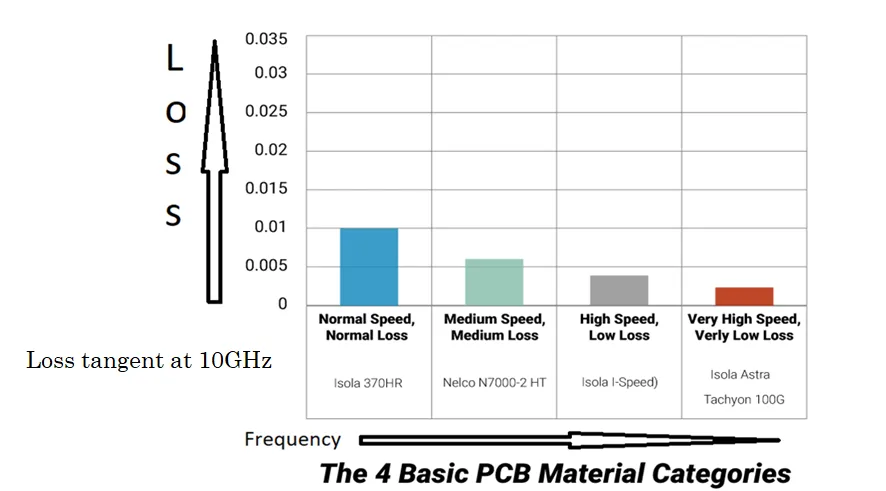
Material selection plays a huge role in RF PCB performance. While standard FR-4 works for lower frequencies, it can introduce significant signal loss above 1 GHz due to its higher dielectric constant (around 4.5) and loss tangent (around 0.02). For better results, consider high-frequency laminates with lower dielectric constants (around 2.2 to 3.5) and loss tangents (below 0.001). These materials ensure minimal signal degradation, especially for applications above 5 GHz.
Work with your prototyping service to select materials that balance performance and cost. Some services offer pre-stocked high-frequency materials for RF PCB quick turn prototype orders, reducing lead times.
3. Leverage Quick-Turn Prototyping Services
Speed is essential in RF PCB prototyping, especially when you’re racing against tight deadlines. An RF PCB quick turn prototype service can deliver bare boards or assembled prototypes in as little as 24 to 48 hours. At ALLPCB, we specialize in rapid turnaround without compromising on quality. Our streamlined process ensures that your RF designs are fabricated and assembled with precision, helping you move from concept to testing in record time.
When choosing a service, look for providers with experience in RF applications. They should offer capabilities like controlled impedance manufacturing, tight tolerances (e.g., ±10% impedance variation), and support for high-frequency materials.
4. Streamline RF PCB Prototype Assembly
Assembly is a critical step in RF PCB prototype assembly. Poor soldering or component placement can introduce parasitic effects that degrade RF performance. To avoid this, ensure your design includes clear assembly instructions, such as specific soldering profiles for RF connectors or sensitive components like LNAs (low-noise amplifiers).
Partner with a prototyping service that offers in-house assembly to minimize delays. Automated assembly processes, such as pick-and-place machines, ensure consistent component placement, which is vital for maintaining signal integrity in RF designs. Additionally, request post-assembly inspections to catch issues like cold solder joints or misaligned components before testing.
Understanding RF PCB Prototype Cost Factors
The RF PCB prototype cost can vary widely depending on several factors. Understanding these can help you budget effectively and avoid surprises. Here are the main elements that influence cost:
- Material Choice: High-frequency laminates are more expensive than standard FR-4. For a small prototype board (e.g., 100 mm x 100 mm), material costs can range from $10 to $50 or more per board, depending on the laminate.
- Layer Count: RF designs often require multiple layers for grounding and signal separation. Each additional layer increases fabrication costs by approximately 20-30%.
- Turnaround Time: Expedited services for quick-turn prototypes come at a premium. A 24-hour turnaround might cost 50-100% more than a standard 5-7 day lead time.
- Assembly Services: If you opt for RF PCB prototype assembly, costs will include labor, component sourcing, and testing. Assembly for a small batch of RF boards can range from $50 to $200, depending on complexity.
- Testing Requirements: Specialized RF testing, such as impedance or signal integrity checks, may add to the overall cost if performed by the prototyping service.
To keep costs down, start with a minimal design for initial prototypes and scale up as needed. Also, consider batching multiple designs into a single order to reduce per-unit fabrication expenses.
Effective Methods for RF PCB Prototype Testing
Testing is the cornerstone of RF PCB prototype testing. Without thorough validation, you risk moving flawed designs into production. Here are some proven methods to ensure your RF prototype performs as expected:
1. Impedance Testing
Use a vector network analyzer (VNA) to measure the impedance of your transmission lines. Ensure they match the target value (e.g., 50 ohms) within a tight tolerance of ±5%. Deviations can cause signal reflections, leading to poor performance. Most prototyping services can provide impedance test reports if requested during fabrication.
2. Signal Integrity Analysis
Evaluate signal integrity by measuring parameters like insertion loss, return loss, and crosstalk. For a 5 GHz signal, insertion loss should ideally be below 1 dB per inch of trace length on high-frequency materials. Use an oscilloscope or spectrum analyzer to observe signal behavior under real-world conditions.
3. Functional Testing
Simulate the operating environment of your RF PCB by connecting it to the intended system. For example, if you’re prototyping a 2.4 GHz antenna module, test it with a compatible transceiver to measure range, data rate, and error rates. This step confirms that your design meets practical performance goals.
4. Thermal and Environmental Testing
RF components can be sensitive to temperature changes and environmental factors. Subject your prototype to thermal cycling (e.g., -40°C to 85°C) to ensure stability. Also, test for moisture resistance if your application involves outdoor use.
Benefits of Partnering with an RF PCB Prototyping Service
Working with a dedicated RF PCB prototyping service offers several advantages, especially for engineers under tight schedules or with limited in-house resources. Here’s why partnering with a provider like ALLPCB makes sense:
- Speed: Quick-turn services deliver prototypes in 24-48 hours, allowing for rapid design iterations.
- Expertise: Experienced providers understand RF-specific requirements like controlled impedance and material selection, reducing the risk of errors.
- Cost Efficiency: Access to bulk materials and advanced manufacturing tools lowers per-unit costs compared to in-house prototyping.
- End-to-End Support: From design review to assembly and testing, a full-service provider streamlines the entire process.
Tips for a Successful RF PCB Prototyping Process
To wrap up, here are some actionable tips to ensure your RF PCB prototyping goes smoothly:
- Start with a clear design specification, including frequency range, impedance, and performance goals.
- Collaborate closely with your prototyping service to select the right materials and manufacturing options.
- Prioritize critical tests like impedance and signal integrity before moving to functional or environmental testing.
- Keep initial prototypes simple to minimize RF PCB prototype cost and focus on validating core functionality.
- Document all test results and design changes to maintain a clear record for future iterations.
Conclusion
RF PCB prototyping is a vital step in developing high-frequency applications, and with the right techniques, you can achieve fast, efficient, and reliable results. By optimizing your design, choosing appropriate materials, leveraging quick-turn services, and conducting thorough RF PCB prototype testing, you’ll be well on your way to validating your concepts and moving toward production. At ALLPCB, we’re committed to supporting engineers with top-tier RF PCB prototyping service solutions, including RF PCB quick turn prototype options and expert assembly. Let us help you turn your RF designs into reality with speed and precision.