 ALLPCB


If you're dealing with a PCB test impedance failure, struggling to fix common PCB design errors, or trying to resolve impedance issues on your printed circuit board, you're in the right place. In this guide, we'll walk you through the essentials of PCB impedance troubleshooting, offering practical solutions to identify and correct problems. From understanding why impedance matters to step-by-step fixes for design flaws, this blog will help you ensure signal integrity and avoid costly mistakes.
Impedance issues can disrupt signal performance, leading to data loss, noise, or complete system failures in high-speed circuits. Whether you're a beginner or an experienced engineer, mastering impedance control is key to reliable PCB designs. Let’s dive into the details of troubleshooting and fixing these challenges with actionable tips and insights.
What Is PCB Impedance and Why Does It Matter?
Impedance in a PCB refers to the resistance to alternating current (AC) signals as they travel through traces, influenced by factors like trace width, dielectric material, and layer stack-up. Measured in ohms (Ω), it’s critical for maintaining signal integrity, especially in high-speed digital circuits where signals switch at rates of 1 GHz or higher.
Why does impedance matter? Mismatched impedance can cause signal reflections, leading to data errors or noise. For example, if a trace is designed for 50Ω impedance but measures at 60Ω due to manufacturing variations, reflections can degrade signal quality by up to 20% or more, depending on the frequency. This is a common cause of PCB test impedance failure in applications like USB, HDMI, or DDR memory circuits.
Understanding and controlling impedance ensures that signals travel without distortion, which is vital for modern electronics. In the sections below, we’ll explore how to spot impedance issues and fix them effectively.
Common Causes of PCB Impedance Failures
Before diving into troubleshooting, let’s identify the root causes of impedance failures. Knowing what leads to these issues will help you prevent them in future designs and resolve existing problems.
- Incorrect Trace Geometry: Trace width and spacing directly affect impedance. For instance, a trace designed to be 5 mils wide for 50Ω impedance might end up at 4.5 mils due to etching inconsistencies, raising impedance by 5-10Ω.
- Dielectric Material Variations: The dielectric constant (Dk) of your PCB substrate impacts impedance. A material rated at Dk=4.5 might vary to 4.7 across batches, shifting impedance by a few ohms.
- Layer Stack-Up Errors: Incorrect spacing between layers or mismatched reference planes can disrupt impedance. A ground plane too far from a signal layer might increase impedance beyond the target value.
- Manufacturing Tolerances: Etching undercuts or over-etching during fabrication can alter trace dimensions, leading to impedance mismatches of up to 15% in extreme cases.
- Signal Frequency Issues: At higher frequencies (above 500 MHz), skin effect and dielectric losses become significant, altering effective impedance if not accounted for in design.
These issues often result in PCB test impedance failure during validation. Identifying the specific cause is the first step to fixing the problem.
Step-by-Step Guide to PCB Impedance Troubleshooting
Troubleshooting impedance issues requires a systematic approach. Below, we outline a clear process to diagnose and resolve impedance PCB problems, ensuring your design performs as intended.
Step 1: Verify Design Specifications
Start by reviewing your design files. Check the target impedance (e.g., 50Ω for single-ended traces or 100Ω for differential pairs) and ensure that trace widths, spacing, and stack-up match the intended values. Use impedance calculators or simulation tools to confirm theoretical values. For example, a 50Ω microstrip trace on FR-4 material with a dielectric thickness of 10 mils typically requires a width of around 18-20 mils, depending on the exact Dk value.
If your design specs are off, this is a common PCB design error that needs correction before moving forward.
Step 2: Perform Impedance Testing
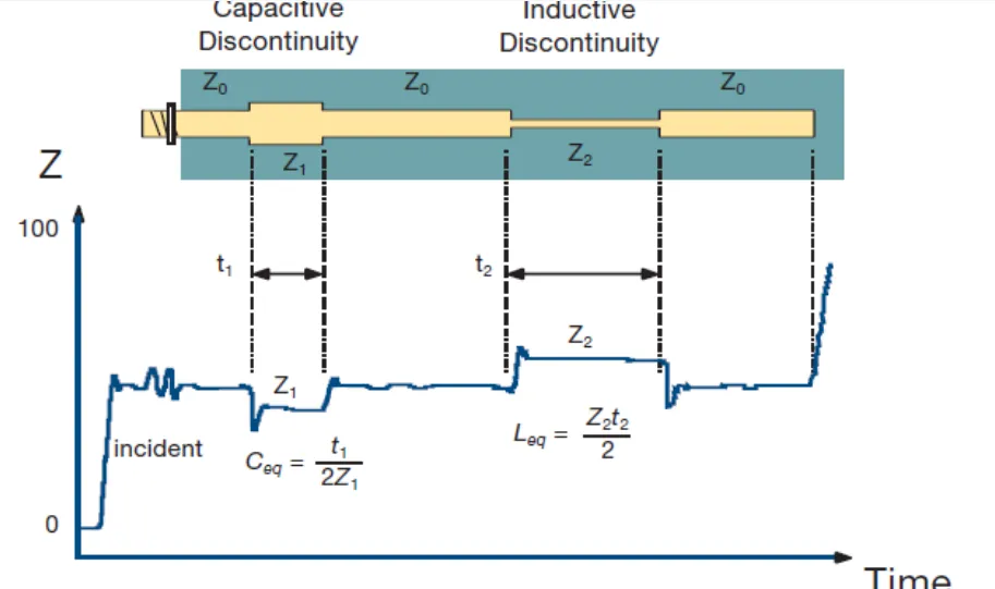
Use a Time Domain Reflectometer (TDR) to measure the actual impedance of traces on your fabricated PCB. A TDR sends a fast pulse down the trace and measures reflections to calculate impedance. If you target 50Ω but measure 58Ω, you’ve identified a PCB test impedance failure. Note the locations of mismatches, as they often point to specific design or manufacturing issues.
For smaller setups without TDR equipment, a vector network analyzer (VNA) can also measure impedance by analyzing signal return loss at various frequencies.
Step 3: Inspect Manufacturing Quality
Examine the physical board for manufacturing defects. Look for uneven trace widths or over-etched areas using a microscope or high-resolution imaging. Cross-sectioning the PCB can reveal dielectric thickness variations or layer misalignment. If traces are consistently narrower than designed (e.g., 4.8 mils instead of 5 mils), work with your fabricator to adjust etching processes for future batches.
Step 4: Simulate and Compare Results
Use simulation software to model your PCB design and compare simulated impedance with measured values. Tools can help identify whether the issue lies in trace geometry, material properties, or stack-up. For instance, if simulations show 50Ω but measurements show 55Ω, the discrepancy likely comes from manufacturing tolerances or material variations.
Step 5: Adjust Design or Fabrication Parameters
Based on your findings, tweak your design to fix common PCB design errors. Widen traces slightly if impedance is too high, or adjust dielectric thickness in the stack-up. If the issue is manufacturing-related, provide tighter tolerances to your fabricator, such as requesting trace width accuracy within ±0.2 mils instead of ±0.5 mils.
After making changes, re-test the board to confirm that impedance falls within the target range (e.g., 50Ω ±5%). This iterative process ensures you resolve impedance PCB issues effectively.
How to Fix Common PCB Design Errors for Impedance Control
Many impedance failures stem from preventable design mistakes. Below are actionable tips to fix common PCB design errors and achieve consistent impedance control.
1. Use Accurate Impedance Calculators
Always calculate trace dimensions using reliable impedance calculators before routing. Input parameters like dielectric constant (typically 4.2-4.5 for FR-4), trace thickness (often 1 oz copper or 1.4 mils), and layer spacing. This prevents basic errors in trace width or spacing that lead to impedance mismatches.
2. Maintain Consistent Reference Planes
Ensure signal traces have a continuous ground or power plane as a reference. Breaks or splits in reference planes can cause impedance to spike by 10-20Ω, disrupting signal integrity. Route high-speed signals away from plane edges to avoid this issue.
3. Account for Manufacturing Tolerances
Design with fabrication limits in mind. If your fabricator’s etching tolerance is ±10%, design traces slightly wider or narrower to compensate for potential variations. For a 50Ω trace, aim for a design value of 48-52Ω to stay within spec after manufacturing.
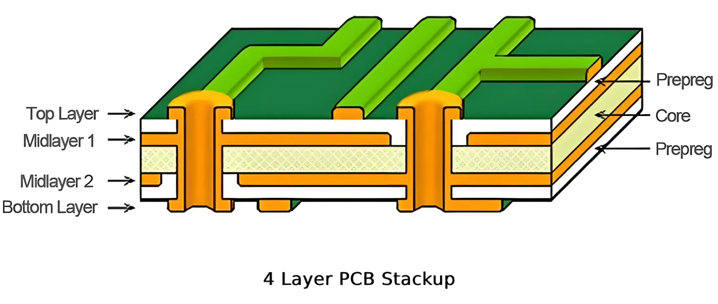
4. Optimize Layer Stack-Up
Work with your fabricator to define a stack-up that supports your impedance targets. For example, placing high-speed signal layers closer to ground planes (e.g., 5-8 mils spacing) reduces impedance variations compared to thicker separations (15-20 mils).
5. Minimize Via Effects
Vias introduce impedance discontinuities, especially in high-speed designs. Use back-drilling to remove unused via stubs, or design with blind vias to keep signal paths short. This can reduce impedance fluctuations by up to 5Ω at critical points.
Preventing PCB Impedance Issues in Future Designs
While troubleshooting fixes immediate problems, prevention saves time and cost in the long run. Here are strategies to avoid PCB test impedance failure before it happens.
- Collaborate Early with Fabricators: Share your impedance requirements (e.g., 50Ω ±5%) with your manufacturer during the design phase. They can recommend materials and processes to meet your specs.
- Specify Materials Clearly: Choose PCB substrates with tight dielectric constant tolerances (e.g., ±0.1 Dk variation) to minimize impedance drift.
- Simulate Before Fabrication: Run full-board simulations to catch impedance issues in the design stage. This can identify mismatches before you even order prototypes.
- Test Prototypes Thoroughly: Always measure impedance on early prototypes using TDR or VNA tools. Use these results to refine your design for mass production.
Tools and Resources for Impedance Troubleshooting
Having the right tools makes troubleshooting and resolving impedance PCB issues much easier. Here are some essentials for engineers:
- Time Domain Reflectometer (TDR): Measures impedance along traces with high precision, ideal for locating mismatches.
- Vector Network Analyzer (VNA): Analyzes signal behavior across frequencies, useful for high-speed designs above 1 GHz.
- Simulation Software: Tools for modeling impedance help predict issues before fabrication, saving time and cost.
- Impedance Calculators: Free online calculators or built-in features in design software provide quick estimates for trace dimensions.
Investing in these tools or partnering with a service provider for testing can significantly improve your ability to fix common PCB design errors.
Conclusion: Mastering PCB Impedance for Reliable Designs
PCB impedance troubleshooting doesn’t have to be a daunting task. By understanding the causes of PCB test impedance failure, following a structured approach to diagnose issues, and applying fixes for common PCB design errors, you can resolve impedance PCB challenges with confidence. Whether it’s adjusting trace geometry, refining your layer stack-up, or collaborating closely with your fabricator, the solutions are within reach.
Impedance control is a cornerstone of high-speed PCB design. With the tips and strategies outlined in this guide, you’re equipped to tackle mismatches, prevent future failures, and ensure signal integrity in your projects. Keep testing, simulating, and iterating on your designs to achieve consistent, reliable results every time.
For more insights on optimizing your PCB designs, stay tuned to our blog. We’re here to help you navigate the complexities of modern electronics with practical advice and expert guidance.


