 ALLPCB


Measuring PCB impedance at home is a practical skill for hobbyists and engineers looking to ensure signal integrity in their designs. Whether you're working on a DIY project or testing a prototype, understanding how to measure PCB impedance can save you time and improve performance. In this guide, we'll walk you through simple, affordable methods for DIY PCB impedance measurement, perfect for home lab PCB testing. Using affordable PCB impedance testing methods, you can achieve reliable results without breaking the bank. Let's dive into the step-by-step process to help you get started.
What Is PCB Impedance and Why Does It Matter?
PCB impedance refers to the resistance to the flow of alternating current (AC) in a circuit, influenced by factors like trace width, dielectric material, and frequency. It’s a critical parameter in high-speed digital and RF circuits because mismatched impedance can cause signal reflections, leading to data loss or interference. For instance, a typical target impedance for many high-speed designs is around 50 ohms, which ensures minimal signal distortion.
Impedance mismatches can degrade performance, especially in applications like USB, HDMI, or Ethernet, where signal integrity is key. By measuring and controlling impedance in your PCB design, you ensure that signals travel efficiently without unwanted noise or delays. For home lab enthusiasts, learning to measure impedance is a valuable step toward creating professional-grade boards.
Tools You’ll Need for DIY PCB Impedance Measurement
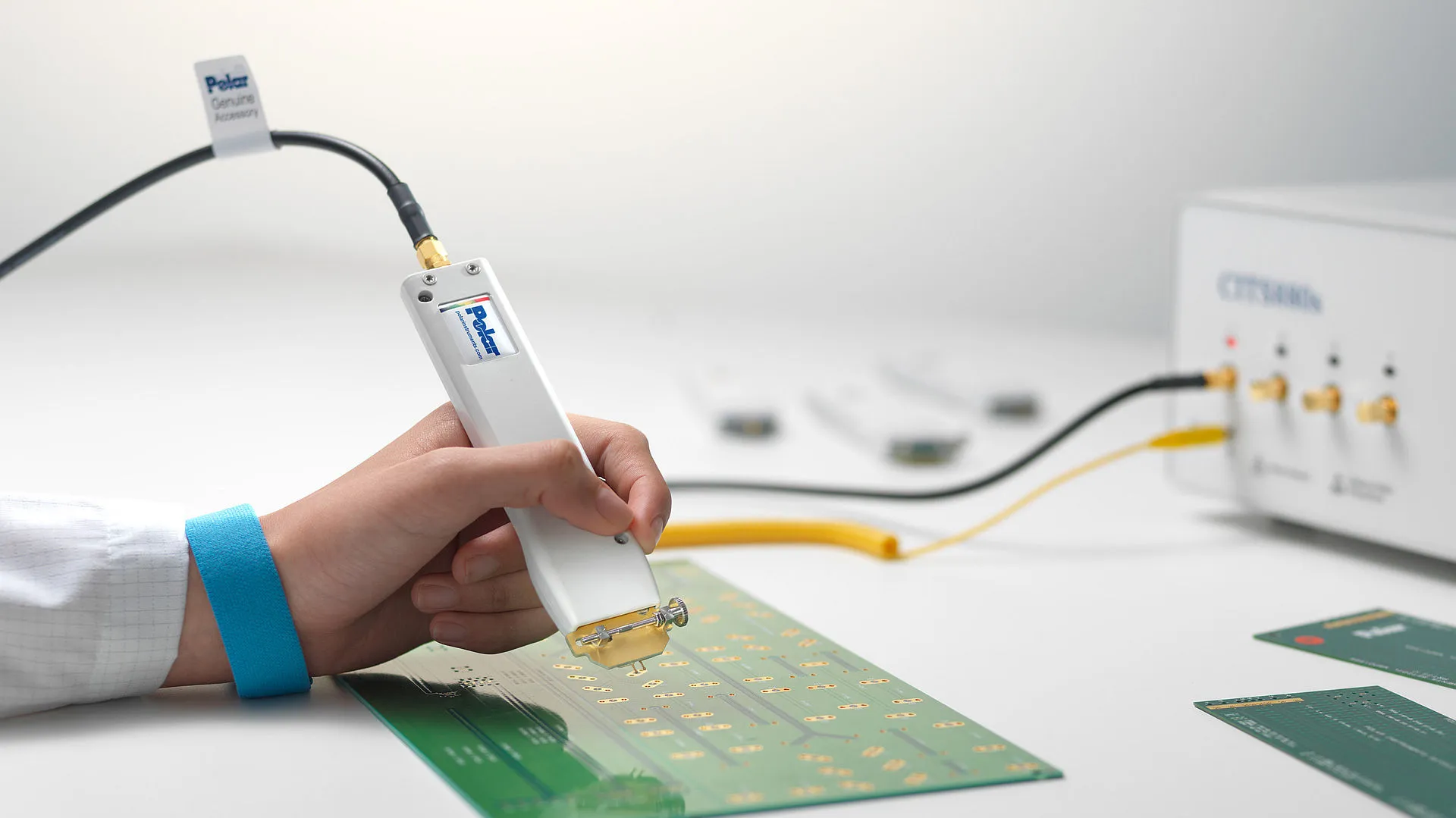
Before we get into the steps, let’s gather the tools required for home lab PCB testing. You don’t need expensive equipment to start; many affordable options work well for basic measurements. Here’s a list of essentials:
- Oscilloscope: A basic digital oscilloscope with a bandwidth of at least 100 MHz can help measure signal behavior. Models in the $200–$400 range are often sufficient for hobbyists.
- Signal Generator: This device sends a known signal through your PCB trace for testing. Affordable ones start at around $50.
- Multimeter: Useful for basic resistance checks and continuity testing.
- BNC Cables and Probes: These connect your tools to the PCB for accurate measurements.
- Termination Resistors: A set of resistors (e.g., 50 ohms) to match the expected impedance and prevent reflections.
- PCB Test Board or Prototype: The board you’re measuring, ideally with accessible test points or vias.
With these tools, you can perform affordable PCB impedance testing methods without investing in professional-grade equipment. If you’re on a tight budget, consider borrowing or renting an oscilloscope from a local maker space.
Understanding the Basics of Impedance Measurement
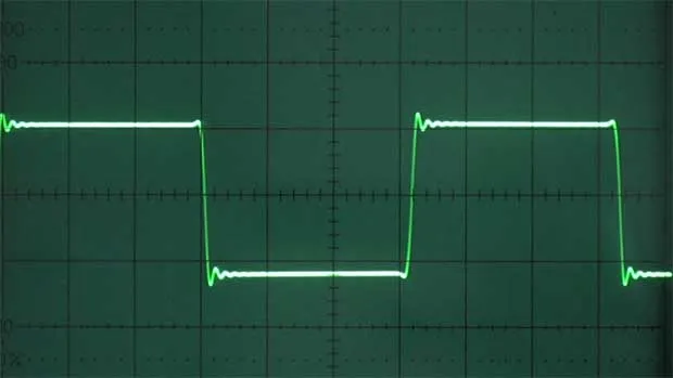
Impedance measurement involves determining how a PCB trace responds to a high-frequency signal. The most common method for hobbyists is the Time Domain Reflectometry (TDR) technique, which uses a fast pulse to detect reflections caused by impedance mismatches. While professional TDR equipment can cost thousands of dollars, you can mimic this process at home using an oscilloscope and a signal generator.
Here’s a quick overview of how it works: When a signal pulse travels along a trace, any change in impedance (like a mismatch) causes part of the signal to reflect back. By measuring the time it takes for the reflection to return and the amplitude of the reflected signal, you can estimate the impedance of the trace. For example, a 50-ohm trace with no mismatch will show minimal reflection, while a mismatch to 75 ohms will create a noticeable reflected wave.
Step-by-Step Guide to Measure PCB Impedance at Home
Now that you understand the concept, let’s walk through the practical steps for DIY PCB impedance measurement. Follow these instructions carefully to get accurate results in your home lab.
Step 1: Prepare Your PCB and Test Setup
Start by ensuring your PCB is ready for testing. If possible, design your board with test points or vias at the start and end of critical traces. This makes it easier to connect probes. Clean the board to remove any dust or residue that could interfere with measurements.
Set up your workspace with all tools within reach. Connect your signal generator to the oscilloscope using a BNC cable, and attach a probe or cable to the PCB trace you want to test. Make sure to ground the setup properly to avoid noise in your readings.
Step 2: Configure the Signal Generator
Set your signal generator to output a square wave or a fast pulse with a rise time of less than 1 nanosecond if possible. The frequency should be in the range of 1–10 MHz, depending on your oscilloscope’s capability and the expected signal speed on your PCB (e.g., USB 2.0 operates at speeds where 5 MHz testing is relevant). This simulates the high-speed signals your board will handle.
Attach a termination resistor (e.g., 50 ohms) at the far end of the trace to minimize reflections during initial setup. This helps establish a baseline for comparison.
Step 3: Connect and Calibrate the Oscilloscope
Connect the oscilloscope probe to the start of the PCB trace. Set the oscilloscope to a time scale that allows you to see the full waveform, typically in the range of 1–10 nanoseconds per division. Adjust the voltage scale to capture the amplitude of the input signal, often around 1 volt peak-to-peak for clarity.
Calibrate the oscilloscope by sending a test signal through a known impedance (like a coaxial cable with a specified impedance of 50 ohms). This helps you understand how a matched impedance looks on the screen—no significant reflections should appear.
Step 4: Measure the Reflected Signal
Remove the termination resistor from the far end of the trace to observe natural reflections. Send the signal pulse through the trace and watch the oscilloscope for any reflected waves. A reflection indicates an impedance mismatch. The time delay between the original pulse and the reflection tells you where the mismatch occurs along the trace, while the amplitude of the reflection indicates the severity of the mismatch.
For a rough calculation, use the formula for characteristic impedance based on the reflection coefficient (ρ):
Z = Z0 * (1 + ρ) / (1 - ρ)
Here, Z0 is the reference impedance (e.g., 50 ohms from your signal generator), and ρ is the ratio of reflected voltage to incident voltage. For example, if the incident voltage is 1V and the reflected voltage is 0.2V, ρ = 0.2, and the impedance Z would be approximately 75 ohms.
Step 5: Analyze and Adjust
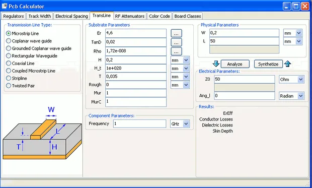
Compare your measured impedance to the target value for your design. If you’re designing for a 50-ohm trace and your measurement shows 75 ohms, you may need to adjust the trace width or dielectric spacing during the design phase. Use online impedance calculators to estimate the required dimensions for your target impedance based on your PCB stack-up (e.g., a 1.6mm FR4 board with a 1oz copper layer).
Repeat the measurement after making changes to confirm that the impedance is closer to your target. This iterative process is key to refining your design.
Alternative Affordable PCB Impedance Testing Methods
If you don’t have access to an oscilloscope or signal generator, there are other affordable PCB impedance testing methods you can try at home. While these may not be as accurate as TDR-based measurements, they can still provide useful insights.
Method 1: Using a Vector Network Analyzer (VNA) Dongle
Low-cost VNA dongles, priced around $50–$100, are becoming popular for hobbyists. These devices connect to your computer via USB and can measure impedance over a range of frequencies (typically 1 MHz to 3 GHz). Software accompanying the VNA will display the impedance directly, making it a user-friendly option for home lab PCB testing. Follow the manufacturer’s instructions to calibrate the device and connect it to your PCB trace for measurement.
Method 2: Resistance Approximation with a Multimeter
For very basic testing, you can use a multimeter to measure the DC resistance of a trace, though this won’t account for high-frequency effects. This method is limited and only useful for identifying major issues like open circuits or shorts. It’s not a true impedance measurement but can be a starting point if you lack other tools.
Common Challenges and How to Overcome Them
Measuring impedance at home comes with challenges, especially with limited equipment. Here are some common issues and tips to address them:
- Noise in Measurements: Ensure proper grounding and keep cables short to reduce interference. Avoid testing near other electronic devices that might emit noise.
- Inaccurate Reflections: Double-check connections and ensure probes are securely attached to test points. Poor contact can skew results.
- Limited Equipment Bandwidth: If your oscilloscope has low bandwidth, test at lower frequencies and extrapolate results cautiously. Understand that high-frequency behavior might differ.
Tips for Improving Impedance Control in PCB Design
Once you’ve measured impedance, you might find mismatches that need correction. Here are practical tips to improve impedance control during the design phase:
- Trace Width and Spacing: Use wider traces for lower impedance and narrower traces for higher impedance. Maintain consistent spacing between traces and ground planes.
- Dielectric Material: Choose a substrate with a known dielectric constant (e.g., FR4 has a dielectric constant of about 4.5). This affects signal speed and impedance.
- Layer Stack-Up: Design your board with ground planes close to signal layers to stabilize impedance. For a 4-layer board, place signal traces on outer layers with ground planes directly beneath.
Conclusion
Measuring PCB impedance at home is entirely achievable with the right tools and techniques. By following the steps outlined in this guide, you can master DIY PCB impedance measurement and ensure your designs meet performance expectations. Whether you’re using an oscilloscope for TDR or a budget-friendly VNA dongle, home lab PCB testing empowers you to tackle high-speed designs without professional equipment. With affordable PCB impedance testing methods, you can refine your skills and build better circuits from the comfort of your workspace.
Start small, experiment with different setups, and iterate on your designs based on your measurements. Over time, you’ll gain confidence in controlling impedance and optimizing signal integrity for any project. Keep learning and refining your approach to create PCBs that perform reliably in real-world applications.


