 ALLPCB


If you're an electrical engineer looking to ensure signal integrity in your printed circuit board (PCB) designs, understanding PCB impedance simulation is critical. How can you accurately simulate and verify impedance control in PCB design? By using specialized PCB impedance simulation software and proven techniques like pre-layout analysis, post-layout verification, and signal integrity checks, you can achieve precise designs that minimize signal distortion and ensure reliability. In this blog, we'll dive deep into the tools, methods, and best practices for simulating signal integrity in PCB design, helping you tackle high-speed design challenges with confidence.
Introduction to PCB Impedance and Signal Integrity
Impedance control is a cornerstone of modern PCB design, especially for high-speed circuits where signal integrity can make or break performance. Impedance mismatches can lead to signal reflections, crosstalk, and timing errors, causing data corruption or system failures. For engineers working on designs with frequencies above 100 MHz, simulating impedance is not just a good practice—it's a necessity.
In this post, we'll explore what PCB impedance simulation entails, the software tools available for accurate analysis, and the techniques you can use to verify impedance control in PCB design. Whether you're designing for telecommunications, automotive, or consumer electronics, these insights will help you achieve reliable and efficient results. Let’s get started with the basics of why impedance matters and how simulation plays a role.

Why Impedance Simulation Matters in PCB Design
Impedance in a PCB refers to the opposition to the flow of alternating current (AC) in a circuit, influenced by factors like trace width, dielectric material, and layer stack-up. For high-speed signals, maintaining a consistent impedance (often 50 ohms or 75 ohms, depending on the application) ensures that signals travel without significant reflection or loss. A mismatch as small as 10% can cause reflections that degrade signal quality, leading to errors in data transmission.
PCB impedance simulation allows engineers to predict and analyze how signals will behave before manufacturing. By identifying potential issues like crosstalk or signal delays during the design phase, you can save time and costs associated with redesigns or failed prototypes. For example, in a 5G communication board operating at 3.5 GHz, even a minor impedance variation can result in significant signal degradation, making simulation an essential step.
Key Tools for PCB Impedance Simulation Software
Choosing the right PCB impedance simulation software is crucial for accurate design. Below are some of the most popular tools that engineers rely on for simulating signal integrity in PCB design, along with their key features.
1. Altium Designer
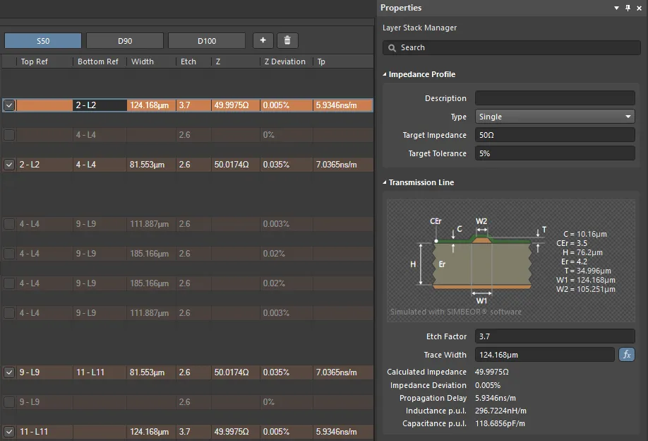
Altium Designer is a widely used tool that offers integrated impedance calculation and signal integrity analysis. Its xSignal feature allows for detailed high-speed design analysis, including impedance control for differential pairs and single-ended traces. Altium’s simulation capabilities help you define stack-up configurations and trace geometries to match target impedance values, often within a tolerance of ±5%.
Practical Tip: Use Altium’s layer stack manager to input dielectric constants and trace dimensions for a 50-ohm controlled impedance line, then run a signal integrity check to verify performance at frequencies up to 10 GHz.
2. Cadence Allegro PCB Designer
Cadence Allegro provides advanced simulation features through its Signal Integrity (SI) tools. It supports pre- and post-layout analysis, enabling engineers to simulate impedance and detect issues like crosstalk or jitter. Cadence also offers integration with Sigrity, a specialized tool for power and signal integrity, making it ideal for complex multi-layer designs.
Example: For a DDR4 memory interface running at 3200 MT/s, Cadence can simulate impedance across multiple layers to ensure timing margins are met, reducing the risk of data errors.
3. ANSYS SIwave
ANSYS SIwave is a powerful tool for electromagnetic simulation, focusing on signal and power integrity. It excels at modeling impedance for high-frequency designs and provides detailed 3D field analysis. SIwave is particularly useful for engineers working on RF or microwave circuits where precise impedance matching (e.g., 50 ohms for RF lines) is critical.
Use Case: In a 24 GHz radar PCB, SIwave can simulate the impedance of microstrip lines and identify parasitic effects that might affect signal quality.
4. HyperLynx by Mentor Graphics
HyperLynx offers robust signal integrity simulation, including impedance analysis for high-speed digital designs. It provides wizards for quick setup of impedance-controlled traces and supports batch simulations to analyze multiple scenarios. HyperLynx is known for its user-friendly interface, making it accessible even for engineers new to simulation.
Practical Tip: Use HyperLynx to simulate a 100-ohm differential pair for a USB 3.0 design, adjusting trace spacing and width to achieve the desired impedance within ±3% tolerance.
Techniques for Simulating Signal Integrity in PCB Design
Beyond selecting the right PCB design software, applying effective techniques is key to verifying impedance control in PCB design. Here are some proven methods to ensure accuracy and reliability in your simulations.
1. Pre-Layout Simulation for Early Impedance Planning
Pre-layout simulation involves analyzing impedance before finalizing the PCB layout. By defining the layer stack-up, trace widths, and spacing early, you can predict impedance values and adjust design parameters accordingly. For instance, a microstrip trace on a standard FR-4 substrate with a dielectric constant of 4.2 might require a width of 7 mils to achieve a 50-ohm impedance.
Steps:
- Define the target impedance based on your application (e.g., 50 ohms for RF, 100 ohms for differential pairs).
- Use simulation software to model the stack-up and trace geometry.
- Adjust parameters like trace width or dielectric thickness to meet the target impedance.
2. Post-Layout Verification for Real-World Accuracy
After completing the layout, post-layout simulation verifies that the actual design matches the intended impedance. This step accounts for real-world factors like manufacturing tolerances and parasitic effects. Tools like Cadence Allegro or HyperLynx can extract the layout geometry and simulate impedance across all critical nets.
Example: In a 10-layer PCB for a server application, post-layout simulation might reveal that a trace near a power plane has an impedance of 53 ohms instead of the target 50 ohms, prompting a redesign of trace spacing.
3. Differential Pair Impedance Control
High-speed designs often use differential pairs (e.g., for USB, HDMI, or Ethernet) that require precise impedance matching, typically 90 or 100 ohms. Simulation tools can model the coupling between traces and ensure consistent impedance. A common issue is uneven spacing, which can cause a mismatch of up to 10 ohms, leading to signal skew.
Tip: Use your simulation software to test different trace separations and edge-coupling configurations to achieve the desired differential impedance within ±5%.
4. Time-Domain Reflectometry (TDR) Simulation
TDR simulation is a technique to measure impedance discontinuities along a trace. By sending a fast pulse and analyzing the reflected signal, you can identify mismatches or abrupt changes in impedance. Many tools like ANSYS SIwave integrate TDR analysis to provide a visual representation of impedance variations.
Use Case: For a PCIe Gen 4 design operating at 16 GT/s, TDR simulation can detect a sudden impedance change at a via transition, allowing you to add stitching vias or adjust the layout for smoother signal flow.
Challenges in PCB Impedance Simulation and How to Overcome Them
While simulation is a powerful tool, it comes with challenges that engineers must address to ensure accurate results.
1. Material Variability
PCB material FR-4 can have variations in dielectric constant (typically ranging from 4.0 to 4.5), affecting impedance calculations. To mitigate this, use manufacturer-provided data for dielectric properties and simulate multiple scenarios to account for tolerances.
2. Manufacturing Tolerances
Etching inaccuracies or layer misalignment during manufacturing can alter trace dimensions, impacting impedance. Work closely with your PCB fabricator to understand their tolerances (e.g., ±10% on trace width) and include these in your simulations.
3. High-Frequency Effects
At frequencies above 1 GHz, skin effect and dielectric loss become significant, altering effective impedance. Use simulation tools that account for frequency-dependent behavior and validate results with real-world testing when possible.
Best Practices for Verifying Impedance Control in PCB Design
To wrap up, here are some best practices to ensure your impedance simulations lead to successful designs:
- Collaborate Early: Work with your PCB manufacturer during the design phase to confirm material properties and fabrication capabilities.
- Iterate and Validate: Run multiple simulations with different parameters to identify the most robust design, then validate with prototypes.
- Document Results: Keep detailed records of simulation settings and results to reference in future projects or troubleshooting.
- Stay Updated: Use the latest versions of PCB impedance simulation software to access improved algorithms and features for signal integrity analysis.
Conclusion: Mastering PCB Impedance Simulation for Better Designs
PCB impedance simulation is an indispensable part of modern PCB design, especially for high-speed applications where signal integrity is paramount. By leveraging powerful PCB impedance simulation software like Altium Designer, Cadence Allegro, ANSYS SIwave, and HyperLynx, and applying techniques such as pre-layout analysis, post-layout verification, and TDR simulation, you can achieve accurate impedance control and reliable performance.
For electrical engineers, mastering these tools and techniques means fewer design iterations, lower costs, and faster time-to-market. Whether you're simulating signal integrity in PCB design for a 5G module or verifying impedance control in a high-speed data interface, the right approach can make all the difference. Start integrating these practices into your workflow today, and take your PCB designs to the next level.


