ALLPCB


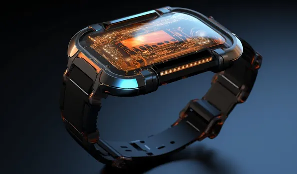
In the fast-evolving world of wearable technology, integrated circuits (ICs) play a vital role in making devices smaller, smarter, and more energy-efficient. However, designing ICs for wearables comes with significant challenges, especially in miniaturization and power efficiency. How do engineers tackle the hurdles of creating tiny, low-power circuits that fit into compact devices like smartwatches and fitness trackers while ensuring long battery life? This blog dives deep into these challenges and explores solutions like low power IC design, miniature IC packaging, and innovations in flexible integrated circuits and wearable PCB design.
The Role of Integrated Circuits in Wearable Technology
Wearable tech, such as fitness bands, medical monitors, and smart clothing, relies heavily on integrated circuits to process data, manage sensors, and connect to other devices. These tiny chips are the brains behind features like heart rate monitoring, step counting, and wireless communication. However, as wearables become smaller and more feature-packed, the demand for compact, efficient ICs grows. Balancing size constraints with performance and power needs is no easy task, especially when devices must run for days on a single charge.
Key Challenges in Miniaturization of ICs for Wearables
Miniaturization is at the heart of wearable technology design. Consumers expect sleek, lightweight devices that are comfortable to wear. This puts pressure on engineers to shrink ICs without sacrificing functionality. Here are the primary challenges in achieving this:
1. Reducing Physical Size Without Losing Performance
The smaller the IC, the harder it is to maintain processing power and reliability. Modern wearables often use System-on-Chip (SoC) designs, where multiple functions like processing, memory, and connectivity are packed into one tiny chip. For instance, some SoCs for wearables measure just 4mm x 4mm but must handle complex tasks. Shrinking transistors to nanoscale levels (e.g., 7nm or 5nm processes) helps, but it also increases design complexity and heat generation.
2. Thermal Management in Compact Designs
Smaller ICs in confined spaces, like those in a fitness tracker, generate heat that can affect performance and user comfort. Without proper heat dissipation, temperatures can rise above safe limits (often exceeding 85°C), risking damage to the chip or surrounding components. Engineers must design ICs with low thermal output and pair them with efficient heat sinks or materials, even in limited space.
3. Signal Integrity in Miniature IC Packaging
As ICs get smaller, maintaining signal integrity becomes tougher. Miniature IC packaging must ensure that high-speed signals (often in the GHz range for Bluetooth or Wi-Fi) aren’t disrupted by noise or interference. This requires precise layout design and advanced packaging techniques like wafer-level packaging (WLP), which reduces the footprint to mere millimeters while protecting signal paths.
Power Efficiency Challenges in IC Design for Wearables
Battery life is a top concern for wearable users. A device that needs daily charging loses its appeal quickly. Designing low power IC design is critical to extending runtime, but it comes with its own set of hurdles:
1. Balancing Performance with Power Consumption
Wearables need to perform tasks like real-time data processing and wireless communication while sipping minimal power. For example, a typical smartwatch IC might consume around 100mW in active mode but must drop to microampere levels (e.g., 3μA) in sleep mode to save energy. Achieving this balance often means using power-gating techniques, where unused parts of the IC are shut off during idle periods.
2. Managing Multiple Sensors and Connectivity
Modern wearables integrate multiple sensors (e.g., accelerometers, gyroscopes, heart rate monitors) and connectivity options like Bluetooth Low Energy (BLE). Each component draws power, and the IC must coordinate them efficiently. Advanced wearable technology components often include dedicated low-power modes for sensors, ensuring they only activate when needed, thus cutting overall consumption.
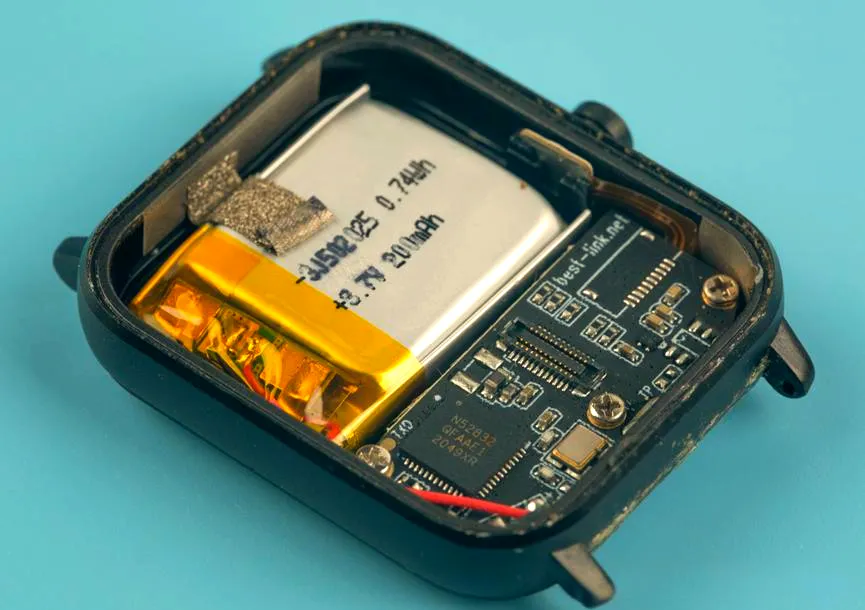
3. Battery Constraints in Small Form Factors
Wearables use tiny batteries, often with capacities below 300mAh. This limits the power budget for ICs. Engineers must optimize every aspect of the circuit, from voltage regulation (e.g., using buck converters with 90% efficiency) to reducing leakage currents in standby mode, which can account for up to 20% of power loss in poorly designed chips.
Innovative Solutions for IC Miniaturization and Power Efficiency
Despite these challenges, advancements in technology are helping engineers overcome barriers in designing ICs for wearables. Here are some cutting-edge solutions:
1. Flexible Integrated Circuits for Wearable Comfort
Traditional rigid ICs don’t always suit wearables, especially those embedded in clothing or skin patches. Flexible integrated circuits made from materials like polyimide or thin silicon can bend and stretch without breaking. These circuits enable designs that conform to the body, improving comfort. For instance, flexible ICs in medical patches can monitor vital signs while maintaining a low profile, often with thicknesses under 0.1mm.
2. Advanced Miniature IC Packaging Techniques
Packaging innovations like chip-scale packaging (CSP) and 3D stacking allow multiple IC layers to be combined in a tiny footprint. CSP can reduce package size by up to 50% compared to traditional methods, making it ideal for wearables. 3D stacking, on the other hand, stacks memory and processing units vertically, saving space while boosting data transfer speeds to over 10Gbps in some designs.
3. Energy Harvesting for Power Efficiency
Energy harvesting is an emerging solution for powering wearables without relying solely on batteries. ICs can be designed to capture energy from body heat, motion, or ambient light. For example, thermoelectric generators integrated into ICs can convert temperature differences (e.g., between skin and air) into small voltages, providing a supplementary power source of up to 100μW per square centimeter.
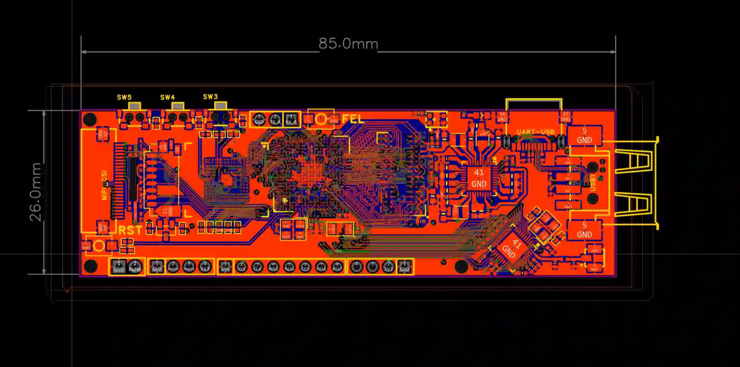
Wearable PCB Design: Supporting IC Integration
ICs don’t work in isolation; they’re mounted on printed circuit boards (PCBs) that must also be optimized for wearables. Wearable PCB design faces similar challenges of size and power, requiring innovative approaches:
1. Flexible and Rigid-Flex PCBs
Flexible PCBs can bend and fold, fitting into irregular shapes within wearables. Rigid-flex designs combine the stability of rigid boards for mounting ICs with flexible sections for connectivity, reducing the overall size. These boards often use high-density interconnects (HDI) with trace widths as small as 50μm to pack more functionality into less space.
2. Component Placement for Efficiency
In wearable PCB design, placing components strategically is key to minimizing power loss and signal delays. For instance, placing power management ICs close to the battery reduces voltage drop across traces, improving efficiency by up to 5%. Similarly, keeping high-speed signal paths short (under 10mm) helps maintain integrity for wireless communication.
3. Thermal and Mechanical Durability
Wearables are exposed to movement, sweat, and temperature changes, so PCBs must be durable. Using materials with low thermal expansion coefficients (e.g., below 15ppm/°C) prevents warping, while conformal coatings protect against moisture. These design choices ensure the ICs and other components remain reliable over time.
Future Trends in ICs for Wearable Technology
The future of ICs in wearables looks promising, with several trends shaping the industry:
- AI Integration: ICs with built-in artificial intelligence can process data locally, reducing power-hungry data transmission to the cloud. This could cut energy use by up to 30% in some applications.
- Ultra-Low-Power Nodes: Next-generation ICs using 3nm or smaller process nodes will push power efficiency further, with leakage currents dropping below 1nA in sleep mode.
- Biocompatible Materials: For medical wearables, ICs made from biocompatible materials will enable long-term implantation or skin contact without adverse reactions.
How ALLPCB Supports Wearable Tech Development
At ALLPCB, we understand the unique demands of designing and manufacturing components for wearable technology. Our expertise in high-precision PCB fabrication and assembly ensures that your wearable technology components meet the strict requirements of size, flexibility, and reliability. Whether you need support for flexible integrated circuits or complex wearable PCB design, our streamlined services help bring your innovative ideas to life with fast turnaround times and top-quality results.
Conclusion: Overcoming Challenges for Smarter Wearables
Integrated circuits are the backbone of wearable tech, but their design is fraught with challenges in miniaturization and power efficiency. From shrinking chip sizes with miniature IC packaging to optimizing energy use through low power IC design, engineers are pushing boundaries to meet consumer demands. Innovations like flexible integrated circuits and advanced wearable PCB design are paving the way for more comfortable, efficient, and powerful devices. As technology advances, the future of wearables will only get smarter, smaller, and more sustainable.
By staying ahead of these challenges and leveraging cutting-edge solutions, the wearable tech industry continues to grow, offering endless possibilities for health, fitness, and connectivity. Trust partners like ALLPCB to support your journey in creating the next generation of wearable devices with precision and innovation.