 ALLPCB


Designing a multi-layer navigation PCB for complex systems can be a challenging yet rewarding task. Whether you're working on GPS modules, autonomous vehicles, or advanced avionics, a well-designed multi-layer PCB ensures reliable performance, signal integrity, and power efficiency. In this comprehensive guide, we'll walk you through the essential steps and strategies to create a high-density PCB design for navigation systems. From layer stackup to routing techniques, we’ve got you covered with actionable insights and practical tips tailored for engineers and designers.
Why Multi-Layer Navigation PCBs Are Essential for Complex Systems
Navigation systems often involve intricate circuitry, high-speed signals, and multiple components packed into a compact space. A single-layer or double-layer PCB simply cannot handle the demands of such systems. Multi-layer navigation PCBs, typically ranging from 4 to 12 layers or more, provide the necessary space for routing, grounding, and power distribution while minimizing electromagnetic interference (EMI). These boards are critical for maintaining signal and power integrity in high-density designs, ensuring that navigation data is processed accurately and efficiently.
In the sections below, we’ll dive deep into the key aspects of designing a multi-layer navigation PCB, including layer stackup, signal and power integrity, and routing strategies. Let’s get started with the foundation of any multi-layer design: the layer stackup.
Navigation PCB Layer Stackup: Building a Solid Foundation
The layer stackup is the blueprint of your multi-layer navigation PCB. It defines how the layers are arranged and what functions each layer serves. A well-planned stackup is crucial for managing signal integrity, reducing noise, and ensuring efficient power distribution in complex navigation systems.
Key Considerations for Layer Stackup Design
- Layer Count: Navigation PCBs often require 4 to 8 layers for moderate complexity, while highly advanced systems may need 12 or more. The number of layers depends on the component density and routing requirements.
- Signal Layers: Place high-speed signal traces on outer layers or near ground planes to minimize crosstalk. For instance, differential pairs used in GPS receivers should be routed on adjacent signal layers for controlled impedance, typically targeting 50 ohms for single-ended signals or 100 ohms for differential pairs.
- Ground Planes: Dedicate at least one or two layers to continuous ground planes. These layers act as a reference for signals and help shield against EMI, which is critical for navigation systems operating in noisy environments.
- Power Planes: Allocate internal layers for power distribution to ensure stable voltage levels. Split power planes if your system requires multiple voltage levels, such as 3.3V for digital circuits and 5V for analog components.
- Dielectric Thickness: The thickness of the dielectric material between layers affects impedance and signal speed. For high-frequency navigation signals (e.g., 1.5 GHz for GPS L1 band), a dielectric constant of around 4.2 (common for FR-4 material) and a thickness of 0.2 to 0.4 mm between signal and ground layers can help maintain signal integrity.
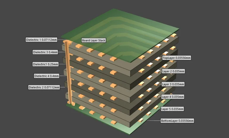
Common Stackup Example for a 6-Layer Navigation PCB
Here’s a typical 6-layer stackup for a navigation PCB:
- Top Layer: High-speed signal traces and components
- Layer 2: Ground plane
- Layer 3: Power plane (e.g., 3.3V)
- Layer 4: Power plane (e.g., 5V)
- Layer 5: Ground plane
- Bottom Layer: Additional signal traces or low-speed I/O
This configuration ensures that signal layers are adjacent to ground planes for better noise reduction and controlled impedance. Always simulate your stackup using design software to verify impedance values before finalizing the design.
Navigation PCB Signal and Power Integrity: Ensuring Reliable Performance
Signal and power integrity are at the heart of any multi-layer navigation PCB design. Navigation systems process high-frequency signals and require stable power delivery to avoid data corruption or system failures. Let’s break down how to achieve both.
Maintaining Signal Integrity
Signal integrity refers to the quality of electrical signals as they travel through the PCB. Poor signal integrity can lead to errors in navigation data, such as incorrect GPS coordinates or delayed sensor readings.
- Controlled Impedance: Match the impedance of traces to the source and load. For example, a 50-ohm impedance is standard for RF signals in navigation systems. Use trace width calculators to determine the appropriate width (e.g., 0.3 mm for a 50-ohm trace on a 1.6 mm FR-4 board).
- Minimize Crosstalk: Keep high-speed traces at least 3 times the trace width apart to reduce interference. Route differential pairs for navigation signals (e.g., I2C or SPI for sensor communication) with equal lengths to avoid timing skew.
- Via Placement: Excessive vias can introduce inductance and signal reflections. Use blind or buried vias for high-density designs to keep signal paths short, especially for frequencies above 1 GHz.
- Termination: Add termination resistors (e.g., 50 ohms for RF lines) near the load to prevent signal reflections in high-speed navigation circuits.
Ensuring Power Integrity
Power integrity ensures that all components receive clean and stable voltage without fluctuations or noise, which is vital for sensitive navigation ICs and sensors.
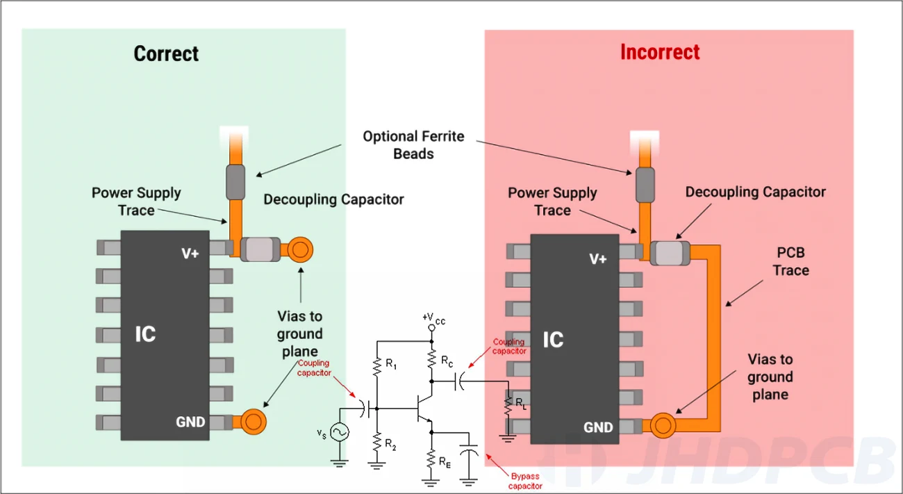
- Decoupling Capacitors: Place decoupling capacitors (e.g., 0.1 μF and 1 μF) close to power pins of ICs to filter high-frequency noise. For a navigation processor, position these capacitors within 2 mm of the pin for optimal effect.
- Power Plane Design: Use solid power planes with minimal cuts to reduce voltage drops. Ensure via connections to power planes are sufficient to handle current demands (e.g., 1A for a GPS module).
- Thermal Management: Navigation systems often include power-hungry components. Add thermal vias under high-power ICs to dissipate heat to inner layers or a heatsink.
Navigation PCB Routing Strategies for High-Density Designs
Routing is one of the most critical stages in designing a multi-layer navigation PCB. High-density PCB design for navigation requires careful planning to accommodate numerous traces, components, and vias in a limited space while maintaining performance.
General Routing Tips
- Prioritize Critical Signals: Route high-speed and sensitive signals first, such as RF traces for GPS antennas or differential pairs for data communication. Keep these traces as short and direct as possible.
- 45-Degree Angles: Use 45-degree angles for trace bends instead of 90-degree turns to reduce signal reflections and EMI.
- Layer Segregation: Separate analog and digital signals on different layers to prevent interference. For example, keep analog sensor signals on the top layer and digital signals on internal layers near a ground plane.
- Ground Stitching: Add stitching vias around the board’s edges to connect all ground planes, creating a low-impedance return path for signals and reducing EMI.
High-Density Routing Techniques
Navigation PCBs often involve tight component placement, making high-density routing a necessity. Here are some strategies to manage this complexity:
- Fanout Planning: For BGA (Ball Grid Array) components commonly used in navigation processors, plan fanout patterns in advance. Route inner pins to inner layers using microvias to save space on outer layers.
- Trace Spacing: In high-density areas, reduce trace spacing to the minimum allowed by your manufacturing process (e.g., 0.1 mm for advanced fabrication). However, maintain adequate spacing for high-voltage traces to avoid arcing.
- Blind and Buried Vias: Use blind vias (connecting outer to inner layers) and buried vias (connecting inner layers only) to free up routing space on outer layers. These are especially useful for routing under dense components.
- Autorouting with Manual Adjustments: While autorouting tools can help with initial trace placement, manually adjust critical paths to optimize signal integrity and avoid congestion.
Design Tools and Simulation for Multi-Layer Navigation PCBs
Modern PCB design software plays a vital role in creating multi-layer navigation PCBs. These tools help simulate layer stackups, calculate impedance, and identify potential issues before manufacturing.
- Stackup Simulation: Use tools to simulate your layer stackup and verify impedance values for high-speed traces. Adjust dielectric thickness and trace width based on simulation results.
- Signal Integrity Analysis: Run signal integrity simulations to detect crosstalk, reflections, and timing issues. Fix these issues by adjusting trace lengths or adding termination components.
- Thermal Analysis: Simulate heat distribution to ensure that high-power components in navigation systems don’t overheat. Add thermal vias or copper pours as needed.
By leveraging these tools, you can catch design flaws early, saving time and cost during prototyping and production.
Manufacturing Considerations for Multi-Layer Navigation PCBs
Once your design is complete, it’s time to prepare for manufacturing. Multi-layer navigation PCBs have specific requirements that must be communicated clearly to ensure a successful build.
- Material Selection: Choose materials like high-frequency laminates (e.g., with a dielectric constant of 3.5 or lower) for RF-heavy navigation designs to minimize signal loss.
- Tolerances: Specify tight tolerances for trace widths and spacing (e.g., ±0.05 mm) to maintain impedance control.
- Panelization: If producing multiple boards, provide panelization guidelines to optimize manufacturing efficiency without compromising board integrity.
- Testing Requirements: Request in-circuit testing (ICT) or flying probe testing to verify signal and power integrity after fabrication.
Work closely with your manufacturing partner to ensure they understand the unique needs of your navigation PCB design, especially for high-density and high-frequency applications.
Conclusion: Mastering Multi-Layer Navigation PCB Design
Designing a multi-layer navigation PCB for complex systems requires careful planning, attention to detail, and a deep understanding of signal and power integrity. By focusing on a well-structured layer stackup, implementing effective routing strategies, and prioritizing high-density design techniques, you can create a reliable and efficient PCB for navigation applications. Whether you’re building a GPS tracker or a sophisticated avionics system, the principles outlined in this guide will help you achieve optimal performance.
Start with a solid foundation by designing your layer stackup, ensure signal and power integrity with proven techniques, and use advanced routing strategies to tackle high-density challenges. With the right tools and manufacturing considerations, your multi-layer navigation PCB will meet the demands of even the most complex systems. Let this guide be your roadmap to success in PCB design for navigation technology.


