ALLPCB


If you're an electrical engineer working on printed circuit board (PCB) design, you've likely wondered how PCB trace width impacts impedance. In short, trace width directly affects the characteristic impedance of a PCB trace—wider traces lower impedance, while narrower traces increase it, influencing signal integrity and performance. This relationship is critical for high-speed designs where impedance matching is key. In this practical guide, we'll dive deep into the PCB trace width impedance relationship, explain how to calculate trace width for desired impedance, and introduce tools like PCB trace impedance calculators to simplify the process.
Introduction: Why PCB Trace Width and Impedance Matter
Designing a PCB isn't just about placing components and routing traces—it's about ensuring signals travel without distortion or loss. Impedance, a measure of opposition to alternating current, plays a huge role in this, especially in high-frequency or high-speed digital circuits. If the impedance isn't controlled, you risk signal reflections, crosstalk, and data errors.
One of the biggest factors affecting impedance is the width of your PCB traces. A mismatch between the trace impedance and the source or load can cause significant issues. Whether you're designing for USB, HDMI, or RF applications, understanding the PCB trace width impedance relationship is essential. In this blog, we'll break down the science behind it, provide actionable tips for calculating trace width for desired impedance, and show you how tools like PCB trace impedance calculators can save time and effort.
What Is Impedance in PCB Design?
Before we dive into trace width, let's clarify what impedance means in the context of PCBs. Impedance, often denoted as Z?, is the total opposition a circuit presents to alternating current. It combines resistance (from the trace material) and reactance (from inductance and capacitance). In PCB design, we usually talk about characteristic impedance, which is the inherent impedance of a transmission line, like a trace, assuming it's infinitely long.
For high-speed signals, maintaining a consistent characteristic impedance (often 50 ohms for RF or 90-100 ohms for differential pairs like USB) is critical to prevent signal reflections. If a trace's impedance doesn't match the source or load, part of the signal bounces back, causing noise and errors. Factors like trace width, thickness, dielectric material, and proximity to ground planes all influence this impedance.
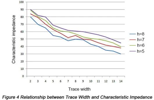
The PCB Trace Width Impedance Relationship
So, how does trace width specifically affect impedance? The relationship is straightforward but critical: as trace width increases, impedance decreases, and vice versa. Here's why:
- Capacitance: A wider trace has more surface area facing the ground plane, increasing the capacitance between the trace and ground. Higher capacitance lowers impedance.
- Inductance: A narrower trace has higher inductance because the magnetic field lines are more concentrated. Higher inductance increases impedance.
For example, in a microstrip configuration (a trace on the top layer over a ground plane), a 10-mil (0.254 mm) wide trace might have a characteristic impedance of 50 ohms on a standard FR-4 substrate with a dielectric constant (Dk) of 4.5 and a height of 1.6 mm. If you widen that trace to 20 mils (0.508 mm), the impedance might drop to around 35 ohms due to increased capacitance. Conversely, narrowing it to 5 mils (0.127 mm) could raise the impedance to 75 ohms or more.
This relationship is crucial in applications like RF design, where 50-ohm impedance is a common standard, or in high-speed digital circuits, where differential pairs often require 90-100 ohms. Adjusting trace width is one of the primary ways to achieve the desired impedance during PCB layout.
Related Reading: The Ultimate Guide to PCB Trace Width for Beginners
Other Factors Influencing Impedance
While trace width is a major player, it's not the only factor affecting impedance. Here are other elements to consider:
- Trace Thickness: Thicker traces reduce resistance but have a minor effect on impedance compared to width. Standard copper thickness is often 1 oz/ft2 (35 μm), but 2 oz/ft2 (70 μm) is used for high-current applications.
- Dielectric Constant (Dk): The material between the trace and ground plane (like FR-4 with Dk ≈ 4.5) affects capacitance. Materials with lower Dk, like Rogers substrates, are used for high-frequency designs to maintain signal integrity.
- Trace Height Above Ground Plane: The distance between the trace and the ground plane impacts capacitance. A smaller height increases capacitance, lowering impedance.
- Trace Length and Routing: While length doesn't directly change characteristic impedance, it affects signal delay and loss, which are related to overall performance.
Understanding how these factors interact with trace width helps you fine-tune your design for optimal performance.
Calculating Trace Width for Desired Impedance
Now that you know the relationship, how do you calculate the trace width for a specific impedance? Doing this manually involves complex equations, but let’s break it down step by step for a microstrip trace, which is common in PCB design.
Step 1: Know Your Target Impedance
Determine the impedance you need. For example, RF designs often require 50 ohms, while differential pairs for USB might need 90 ohms.
Step 2: Gather PCB Parameters
You'll need:
- Dielectric constant (Dk) of your substrate (e.g., 4.5 for FR-4).
- Height of the dielectric (H) between trace and ground plane (e.g., 1.6 mm for a standard 2-layer PCB).
- Copper thickness (T), typically 35 μm for 1 oz copper.
Step 3: Use the Microstrip Impedance Formula
The characteristic impedance (Z?) of a microstrip can be approximated using this formula:
Z? = (87 / √(Dk + 1.41)) * ln(5.98H / (0.8W + T))
Where:
- Z? is the characteristic impedance (ohms)
- Dk is the dielectric constant
- H is the height of the dielectric (in same units as W and T)
- W is the trace width
- T is the trace thickness
This equation is complex to solve for W (trace width) manually, so engineers often use approximations or software tools. For instance, for a 50-ohm impedance on FR-4 (Dk=4.5, H=1.6 mm, T=35 μm), the trace width (W) is roughly 2.9 mm. However, this varies based on exact stack-up and materials.
Step 4: Verify with Simulation or Tools
Manual calculations are prone to error due to simplifications. It's best to verify using PCB design software like Altium Designer, KiCad, or online PCB trace impedance calculators, which account for real-world variables.
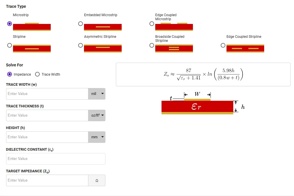
Using a PCB Trace Impedance Calculator
For most engineers, calculating trace width manually is time-consuming and unnecessary thanks to modern tools. A PCB trace impedance calculator simplifies the process by doing the math for you. These calculators are available online or integrated into PCB design software. Here's how to use one:
- Input Parameters: Enter the target impedance (e.g., 50 ohms), dielectric constant (e.g., 4.5), dielectric height (e.g., 1.6 mm), and copper thickness (e.g., 35 μm).
- Select Trace Type: Choose whether it's a microstrip (trace over ground plane) or stripline (trace between two ground planes).
- Get Results: The calculator outputs the required trace width. For instance, for 50 ohms on a 1.6 mm FR-4 board, you might get a width of approximately 2.8-3.0 mm.
Popular free tools include those from AdvancedPCB, MCLPCB, and others mentioned on engineering forums. These tools often allow you to tweak parameters and see how impedance changes with trace width in real-time, making them invaluable for quick iterations.
Related Reading: Understanding PCB Trace Impedance: Factors, Calculations, and Control Techniques
Practical Tips for Controlling Impedance with Trace Width
Here are some actionable tips for electrical engineers to manage impedance through trace width in PCB design:
- Start with Standards: Use industry standards for impedance (e.g., 50 ohms for RF, 100 ohms for differential pairs) as a starting point. Then adjust trace width to match.
- Consult Stack-Up Data: Work with your PCB manufacturer to confirm dielectric constants and layer heights. Small variations in materials can shift impedance by 5-10%.
- Avoid Sharp Corners: When routing traces, use 45-degree angles or curves instead of 90-degree bends to minimize impedance discontinuities.
- Test and Iterate: After calculating trace width, simulate your design using tools like HyperLynx or Ansys to verify performance before fabrication.
- Account for Manufacturing Tolerances: Trace width can vary by ±10% during fabrication. Design with some margin or specify tighter tolerances if impedance is critical.
For example, in a recent project designing a 5G RF board, I needed 50-ohm traces for antenna connections. Using an online PCB trace impedance calculator, I determined a trace width of 2.85 mm for my 2-layer FR-4 board. After simulation, I adjusted to 2.9 mm to account for manufacturing variations, and post-fabrication tests showed impedance within 2% of the target—well within acceptable limits.
Common Mistakes to Avoid
Even experienced engineers can make errors when managing trace width and impedance. Watch out for these pitfalls:
- Ignoring Dielectric Variations: Assuming a fixed Dk (like 4.5 for FR-4) without confirming with your manufacturer can lead to impedance mismatches, as Dk can range from 4.2 to 4.8.
- Overlooking Adjacent Traces: Nearby traces can cause crosstalk, altering effective impedance. Maintain proper spacing (often 3x the trace width) for isolation.
- Neglecting Ground Planes: A broken or poorly designed ground plane can disrupt impedance. Ensure a continuous ground plane beneath critical traces.
Conclusion: Mastering Trace Width for Impedance Control
Understanding how PCB trace width affects impedance is a fundamental skill for any electrical engineer working on high-speed or high-frequency designs. By grasping the PCB trace width impedance relationship, calculating trace width for desired impedance, and leveraging tools like PCB trace impedance calculators, you can ensure signal integrity and avoid costly redesigns.
Remember, wider traces lower impedance, while narrower traces increase it. Use calculators or software to determine the exact width for your target impedance, and always validate with simulations or manufacturer data. With these practices, you'll be well-equipped to tackle even the most demanding PCB projects.
Have questions or tips from your own experience with trace width and impedance? Drop a comment below—we'd love to hear from you! And if you found this guide helpful, share it with fellow engineers to help them master PCB design.