 ALLPCB


If you're diving into DIY electronics projects and wondering how to create a PCB stack-up for simple designs, you're in the right place. A PCB stack-up is the arrangement of layers in a printed circuit board, and for beginners, starting with a single layer PCB or a double layer PCB is often the best approach. In this guide, we'll walk you through the essentials of designing a PCB stack-up for small-scale projects, including home etching techniques. Whether you're building a basic circuit at home or experimenting with more complex ideas, we'll cover everything you need to know to get started with confidence.
What Is a PCB Stack-Up and Why Does It Matter?
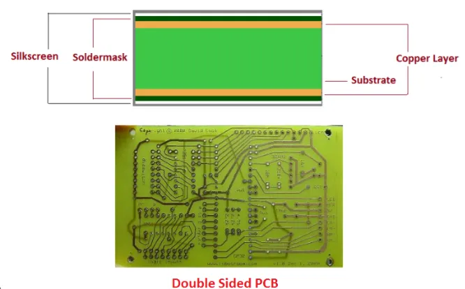
A PCB stack-up refers to the way layers of a printed circuit board are organized. These layers include conductive copper traces, insulating materials, and sometimes ground or power planes. For simple projects, a stack-up might be as basic as a single layer PCB with one copper layer or a double layer PCB with two. The design of your stack-up impacts how well your circuit performs, how easy it is to build, and even how much it costs to produce.
For DIY enthusiasts working on home etching or small electronics projects, understanding stack-up design helps ensure your circuit works as intended. A poorly planned stack-up can lead to issues like signal interference or difficulty in routing traces. By learning the basics, you can avoid common pitfalls and create functional boards even with limited tools and resources.
Single Layer PCB: The Simplest Option for Beginners
A single layer PCB is the most basic type of board, consisting of one layer of conductive copper on top of an insulating substrate, usually made of materials like FR-4. This design is ideal for beginners working on DIY electronics projects because it’s straightforward to design and easy to etch at home.
Advantages of Single Layer PCBs
- Simplicity: With only one layer to worry about, routing traces (the paths that connect components) is much easier. You don’t need to think about vias, which are holes connecting multiple layers.
- Cost-Effective: Single layer boards use fewer materials, making them cheaper to produce or etch at home.
- Perfect for Basic Circuits: If you're building something simple like an LED blinker or a small power supply, a single layer PCB often has enough space for all your components and traces.
Limitations to Keep in Mind
While single layer PCBs are great for starters, they do have drawbacks. If your project has many components or complex connections, you might run out of space for traces. Crossing traces isn’t possible without jumper wires, which can make the board messy and harder to debug.
Double Layer PCB: Stepping Up for More Complexity
A double layer PCB has two layers of copper, one on each side of the insulating substrate. This setup gives you more room to route traces and connect components, making it a great choice for slightly more advanced DIY electronics projects.
Benefits of Double Layer PCBs
- More Routing Space: With two layers, you can route traces on both the top and bottom, using vias to connect them. This is helpful for circuits with more components or connections.
- Better Signal Management: You can dedicate one layer to ground or power, reducing noise and improving performance. For example, in a small audio amplifier project, this can help minimize interference.
- Still DIY-Friendly: While more complex than single layer boards, double layer PCBs can still be etched at home with the right tools and patience.
Challenges of Double Layer Designs
Double layer PCBs are trickier to design and etch. You’ll need to align the top and bottom layers accurately during home etching, and drilling vias by hand can be time-consuming. Additionally, the design process requires software that supports multi-layer layouts to ensure traces don’t overlap incorrectly.
How to Design a PCB Stack-Up for Simple Projects
Designing a PCB stack-up for a simple project doesn’t have to be complicated. Whether you’re working on a single layer PCB or a double layer PCB, follow these steps to create a functional design.
Step 1: Define Your Project Requirements
Start by figuring out what your circuit needs. How many components will you use? Do you need a ground plane to reduce noise? For very basic projects, a single layer PCB might be enough. If you’re building something like a small microcontroller circuit with multiple connections, consider a double layer PCB to keep things organized.
Step 2: Choose the Right Materials
For home etching, you’ll typically use FR-4 boards, which are widely available and affordable. These boards come in standard thicknesses like 1.6mm, which is suitable for most DIY projects. The copper thickness is often 1 oz per square foot (about 35 micrometers), providing enough conductivity for low-power circuits.
Step 3: Plan Your Layer Arrangement
- For a single layer PCB, place all traces and components on one side. Keep traces as short as possible to avoid signal delays or interference.
- For a double layer PCB, decide how to split your traces. A common approach is to use the top layer for signal traces and the bottom for ground or power connections. This setup can help with noise reduction, especially in projects with digital signals switching at speeds above 1 MHz.
Step 4: Use Design Software
To create your PCB layout, use free or open-source design software. These tools let you draw your circuit schematic and then convert it into a PCB layout. Make sure to check the software’s layer settings to match your stack-up (one or two layers). Pay attention to trace widths— for low-current signals, a width of 0.25mm (10 mils) is often enough, but for power lines, use 0.5mm (20 mils) or more to handle currents up to 1A safely.
Home Etching: Crafting Your PCB Stack-Up by Hand
Home etching is a popular method for DIY enthusiasts to create single layer or double layer PCBs without professional equipment. It involves transferring your design to a copper-clad board and using chemicals to remove unwanted copper, leaving behind your traces.
Tools and Materials for Home Etching
- Copper-clad board (single or double-sided, depending on your stack-up)
- Etchant solution (like ferric chloride or a mix of hydrogen peroxide and hydrochloric acid)
- Transfer paper or a permanent marker for manual designs
- Drill for vias (if using a double layer PCB)
- Protective gloves and safety goggles for handling chemicals
Steps for Home Etching a PCB
- Print or Draw Your Design: Use a laser printer to print your PCB layout onto transfer paper, or draw it directly on the board with a marker. For double layer PCBs, print separate designs for top and bottom layers.
- Transfer the Design: Iron the printed design onto the copper board to transfer the toner, or ensure your marker lines are clear and precise.
- Etch the Board: Submerge the board in etchant solution. Agitate gently for 10-20 minutes until the unprotected copper dissolves. For double layer boards, etch one side at a time or protect the other side with tape.
- Clean and Drill: Rinse the board with water, remove the toner or marker with acetone, and drill holes for vias or components as needed.
Safety Tips for Home Etching
Always work in a well-ventilated area when using chemicals. Wear gloves and goggles to protect your skin and eyes from etchant solutions, which can be corrosive. Dispose of used chemicals responsibly, following local regulations.
Tips for Successful PCB Stack-Up in DIY Projects
Creating a PCB stack-up for simple projects can be rewarding, but it takes practice. Here are some tips to help you succeed, especially when working on single layer or double layer PCBs at home.
- Start Small: Begin with a single layer PCB for your first few projects. Once you’re comfortable with the design and etching process, move to double layer boards for more complex circuits.
- Double-Check Your Design: Before etching, review your layout for errors. A misplaced trace or via can ruin a board. Use the design software’s error-checking tools to catch issues like unconnected nets.
- Keep Traces Short and Wide: Shorter traces reduce signal loss, and wider traces (up to 0.5mm for power) handle higher currents better. For example, a trace carrying 500mA should be at least 0.3mm wide to avoid overheating.
- Test Incrementally: After etching, test your board with a multimeter to ensure continuity and check for shorts before soldering components.
Common Mistakes to Avoid in PCB Stack-Up Design
Even simple projects can go wrong if you overlook key details. Here are some pitfalls to watch out for when designing your PCB stack-up or etching at home.
- Overcrowding a Single Layer PCB: Trying to fit too many components on one layer can lead to messy routing or the need for jumper wires. If space is tight, consider upgrading to a double layer design.
- Misaligned Layers in Double Layer PCBs: During home etching, ensure the top and bottom layers align perfectly, especially for vias. Misalignment can make connections impossible.
- Ignoring Trace Clearance: Traces too close together can cause shorts or arcing, especially at voltages above 12V. Maintain a clearance of at least 0.2mm (8 mils) between traces for safety.
Scaling Up: When to Move Beyond Simple Stack-Ups
As your skills grow, you might outgrow single layer and double layer PCBs. If your DIY electronics projects start involving high-speed signals (above 10 MHz) or complex circuits like multi-sensor systems, you’ll need multi-layer boards with more advanced stack-ups. These designs often include dedicated ground planes and power planes to manage impedance, which can be as critical as maintaining 50 ohms for certain high-frequency applications. At this stage, professional manufacturing might be more practical than home etching.
Conclusion: Start Building Your PCB Stack-Up Today
Creating your own PCB stack-up for simple projects is an exciting step in DIY electronics. Whether you choose a single layer PCB for a basic circuit or a double layer PCB for something more advanced, the key is to plan carefully and practice your skills. Home etching offers a hands-on way to bring your designs to life, even with minimal equipment. By following the steps and tips in this guide, you can build functional boards tailored to your projects while avoiding common mistakes.
With each project, you’ll gain confidence in designing and crafting PCBs. Start with a small, manageable design, and soon you’ll be ready to tackle bigger challenges. Grab your tools, pick a simple circuit, and dive into the world of PCB creation today!


