 ALLPCB


Designing a printed circuit board (PCB) layout can be a complex task, but with the right tools and processes, you can achieve a seamless and efficient design. Whether you're working on a simple circuit board layout or a complex multilayer PCB layout, having a structured approach and the best software at your disposal makes all the difference. In this comprehensive guide, we'll walk you through the essential tools and proven processes to streamline your PCB layout design, covering everything from component placement to routing techniques for RF circuit board layouts.
At ALLPCB, we understand the challenges of creating a reliable and high-performing PCB. That’s why we’ve put together this detailed resource to help engineers and designers like you master the design of circuit board layout with practical tips and insights. Let’s dive into the world of PCB layout services and explore how to optimize every step of the process.
What Is PCB Layout and Why Does It Matter?
PCB layout is the process of arranging components and routing traces on a printed circuit board to ensure proper functionality, reliability, and manufacturability. A well-designed PCB layout minimizes issues like signal interference, heat buildup, and manufacturing defects, while a poor layout can lead to performance failures or costly redesigns. Whether you're focusing on multilayer PCB layout or RF circuit board layout, the layout phase is critical to the success of your electronic product.
The design of circuit board layout directly impacts signal integrity, power distribution, and electromagnetic compatibility (EMC). For instance, improper PCB component placement can result in crosstalk or high impedance, especially in high-speed or RF designs where signal speeds can exceed 1 GHz. By following best practices and using advanced tools, you can avoid these pitfalls and create a board that performs as intended.
Essential Tools for Seamless PCB Layout Design
To achieve a flawless PCB layout, you need tools that offer precision, flexibility, and robust features. Here are some key categories of tools that can help with the design of circuit board layout:
1. PCB Design Software
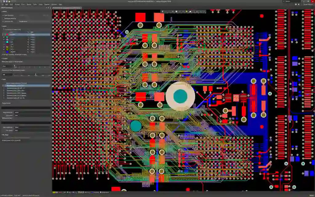
Modern PCB design software is the backbone of any successful layout project. These tools provide schematic capture, component libraries, and advanced routing capabilities to simplify the process. Look for software that supports multilayer PCB layout, offers simulation features for RF circuit board layout, and includes design rule checks (DRC) to catch errors early.
Many of these platforms also integrate with manufacturing processes, ensuring your design is ready for production. Features like 3D visualization help you see how components fit on the board, while auto-routing options can save time on complex designs with hundreds of traces.
2. Simulation and Analysis Tools
Simulation tools are vital for testing your PCB layout before manufacturing. These tools analyze signal integrity, thermal performance, and power distribution to identify potential issues. For RF circuit board layout, simulation software can model high-frequency behavior and ensure impedance matching, often targeting values like 50 ohms for standard RF applications.
Using these tools, you can predict how your design will behave under real-world conditions, reducing the risk of costly revisions. They are especially important for multilayer PCB layout, where inter-layer interference can degrade performance if not addressed.
3. Component Libraries and Footprint Generators
Accurate component footprints are essential for proper PCB component placement. Tools that provide access to extensive libraries or allow you to create custom footprints ensure that your components fit perfectly on the board. This is particularly crucial for RF designs, where precise placement can impact signal quality.
Having a reliable library saves time and reduces errors during the design phase, allowing you to focus on optimizing the layout rather than manually creating footprints.
Key Processes for a Seamless PCB Layout
Beyond tools, following a structured process is critical to achieving a seamless PCB layout. Here’s a step-by-step guide to help you navigate the design of circuit board layout, from initial planning to final checks.
1. Start with a Detailed Schematic
Before diving into PCB layout, create a detailed schematic that defines all connections and components. This blueprint serves as the foundation for your design, ensuring that every element is accounted for during PCB component placement. A clear schematic also helps in generating a netlist, which guides the routing process.
Double-check your schematic for errors, as mistakes at this stage can lead to significant issues later. For multilayer PCB layout, ensure that power and ground planes are clearly defined to avoid signal integrity problems.
2. Define the Board Outline and Constraints
Once your schematic is ready, establish the physical dimensions of your PCB. The board outline should accommodate all components while meeting size constraints for your product. Consider manufacturing limitations, such as minimum trace widths (often as low as 0.1 mm for advanced designs) and spacing rules, to ensure your design is producible.
For RF circuit board layout, pay attention to board material and stack-up, as these factors influence signal propagation and impedance. Using a high-frequency laminate with a dielectric constant around 3.5 can improve performance in RF applications.
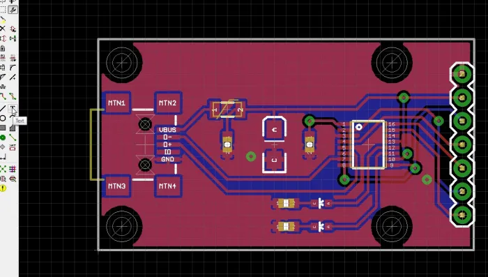
3. Optimize PCB Component Placement
PCB component placement is a critical step that affects both functionality and manufacturability. Place components logically, grouping related parts together to minimize trace lengths and reduce interference. For example, in RF circuit board layout, position sensitive components like amplifiers away from noisy power supplies to avoid signal distortion.
In multilayer PCB layout, distribute components across layers to balance thermal load and signal paths. Keep high-speed components on the top layer to reduce via inductance, which can be as high as 1 nH per via if not managed properly.
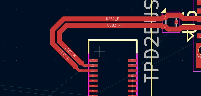
4. Master PCB Routing Techniques
Routing is where your PCB layout truly comes to life. PCB routing techniques determine how signals travel between components, impacting performance and reliability. Here are some best practices to follow:
- Minimize Trace Lengths: Shorter traces reduce signal delay and resistance. For high-speed designs, keep critical traces under 10 mm if possible to maintain signal integrity.
- Use Ground Planes: In multilayer PCB layout, dedicate entire layers to ground planes to provide a low-impedance return path and shield against interference.
- Avoid Sharp Angles: Route traces with 45-degree angles instead of 90-degree turns to prevent signal reflection, especially in RF circuit board layout.
- Differential Pair Routing: For high-speed signals, route differential pairs with matched lengths to avoid timing skew, targeting differences under 0.5 mm.
Advanced routing tools can automate much of this process, but manual adjustments are often necessary for optimal results, particularly in complex designs.
5. Perform Design Rule Checks (DRC)
After completing your layout, run a design rule check to catch errors like overlapping traces, insufficient spacing, or unconnected nets. DRC tools ensure that your design adheres to manufacturing standards, such as minimum clearance of 0.2 mm between traces for standard processes.
For RF circuit board layout, DRC can also verify impedance control and ensure that critical traces meet specific width requirements. Addressing these issues early prevents delays during production.
6. Simulate and Test Before Manufacturing
Before sending your design for fabrication, use simulation tools to test its performance. Check for thermal hotspots, signal integrity issues, and power distribution problems. In multilayer PCB layout, simulate inter-layer crosstalk to ensure signals on adjacent layers don’t interfere with each other.
Testing at this stage can save significant time and cost, as fixing a design error after manufacturing can be 10 times more expensive than catching it during the layout phase.
Special Considerations for Multilayer and RF PCB Layouts
While the general process applies to most PCBs, multilayer PCB layout and RF circuit board layout require additional care due to their complexity.
Multilayer PCB Layout
Multilayer boards, often with 4 to 16 layers, are used in compact, high-density designs. They allow for more components and complex routing but introduce challenges like inter-layer interference and thermal management. Use dedicated power and ground planes to stabilize voltage levels, targeting ripple under 50 mV for sensitive circuits.
Stack-up design is crucial—alternate signal and plane layers to minimize crosstalk. For instance, a common 6-layer stack-up might be Signal-Ground-Signal-Power-Ground-Signal, ensuring shielding between signal layers.
RF Circuit Board Layout
RF designs operate at high frequencies, often above 100 MHz, making them sensitive to layout issues. Impedance matching is critical, with traces designed to maintain 50-ohm impedance for most RF systems. Use microstrip or stripline configurations to control signal paths, and avoid vias in RF lines as they introduce inductance.
Keep RF traces short and straight, and isolate them from digital or power circuits to prevent noise coupling. Materials with low dielectric loss, such as those with a loss tangent below 0.002, are ideal for RF applications.
How PCB Layout Services Can Enhance Your Design
If managing the entire PCB layout process feels overwhelming, professional PCB layout services can provide expert assistance. These services offer access to experienced designers who specialize in multilayer PCB layout, RF circuit board layout, and advanced PCB routing techniques. They ensure that your design meets industry standards and is optimized for performance and manufacturability.
At ALLPCB, we provide comprehensive support for every stage of PCB design, from initial schematic to final layout. Our team uses cutting-edge tools and follows best practices to deliver boards that meet your exact specifications, saving you time and reducing the risk of errors.
Final Tips for a Seamless PCB Layout
To wrap up, here are a few final tips to ensure your PCB layout process is as smooth as possible:
- Always start with a clear plan and schematic to avoid rework.
- Use high-quality tools that support simulation and DRC for error-free designs.
- Pay extra attention to PCB component placement and routing, especially for multilayer and RF designs.
- Collaborate with manufacturing experts early to align your design with production capabilities.
By following these guidelines and leveraging the right tools, you can master the design of circuit board layout and create PCBs that perform reliably in any application. Whether you're a seasoned engineer or just starting out, a structured approach to PCB layout will set you up for success.
At ALLPCB, we’re committed to helping you achieve exceptional results with your PCB projects. Explore our range of services and resources to take your designs to the next level, and experience the difference of a truly seamless PCB layout process.


