 ALLPCB


Are you a beginner looking to turn your electronic ideas into a real, working circuit board? Designing your first PCB (Printed Circuit Board) layout can feel overwhelming, but with the right guidance and tools, it’s easier than you think. In this comprehensive guide, we’ll walk you through every step of creating a beginner PCB layout using a free PCB design software. Whether you’re moving from a breadboard to PCB or exploring single-layer PCB design, this PCB design tutorial will help you bring your project to life with confidence.
Let’s dive into the process of transforming a schematic into a functional PCB using a powerful, no-cost tool that’s perfect for beginners. By the end of this post, you’ll have a clear roadmap for simple PCB layout design and actionable tips to get started with online PCB design or desktop software. Let’s make easy PCB software your gateway to success!
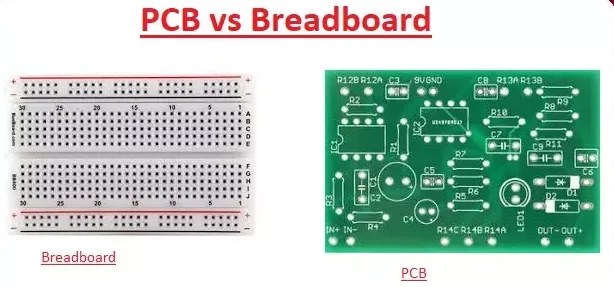
Why Move from Breadboard to PCB?
Before we jump into the step-by-step process, let’s talk about why designing a PCB is worth the effort. Breadboards are great for prototyping and testing ideas, but they’re not ideal for permanent or reliable projects. Wires can come loose, connections may fail, and the setup isn’t compact. A PCB solves these issues by providing a stable, professional, and space-efficient solution for your circuits.
Creating a PCB also allows for better signal integrity, especially in high-frequency designs where breadboard stray capacitance can cause issues (often in the range of 2-10 pF per connection). Plus, it’s a skill that opens doors to more complex projects and even professional opportunities. With free PCB design software, the barrier to entry is lower than ever for beginners.
Getting Started: What You Need for Your First PCB Design
Designing a PCB doesn’t require expensive tools or years of experience. Here’s what you’ll need to begin your journey with beginner PCB layout:
- A Free Design Tool: For this guide, we’ll use a widely accessible, no-cost software that’s beginner-friendly and supports online PCB design or desktop use. This tool offers an intuitive interface and plenty of resources for learning.
- A Basic Schematic: If you’ve already built a circuit on a breadboard, you likely have a rough idea of your design. We’ll start by turning that into a digital schematic.
- Components List: Know the parts you’re using (resistors, capacitors, ICs, etc.) and their specifications, like package sizes (e.g., 0805 for surface-mount resistors).
- Time and Patience: Your first design might take a few hours, but the learning curve gets easier with practice.
With these in hand, you’re ready to dive into the world of simple PCB layout design using easy PCB software.
Step 1: Choose and Install Your Free PCB Design Software
The first step in any PCB design tutorial is selecting the right tool. For beginners, a free PCB design software that balances simplicity with functionality is key. The tool we’re using in this guide is perfect for single-layer PCB design and offers both cloud-based and offline options, making it a great choice for online PCB design.
Download and install the software from its official website, or access the web-based version if available. Most free tools come with built-in libraries of components and tutorials to help you get started. Spend a few minutes exploring the interface—look for the schematic editor and the PCB layout editor, as you’ll use both.
Step 2: Create Your Schematic
Every PCB starts with a schematic—a blueprint of how your components connect. If you’re moving from a breadboard to PCB, sketch out your circuit on paper first if you haven’t already. Then, open the schematic editor in your chosen software.
Here’s how to build your schematic:
- Add Components: Search the software’s library for your components (e.g., a 10kΩ resistor or a 555 timer IC). Drag and drop them onto the workspace.
- Connect Components: Use the wiring tool to draw lines between component pins, matching your breadboard setup. Ensure power (like 5V) and ground connections are clear.
- Label Nets: Assign names to important connections (like “VCC” for power) to keep things organized when you move to the layout phase.
- Check for Errors: Most tools have a design rule check (DRC) feature to spot unconnected pins or other issues. Run it before proceeding.
For a simple LED blinker circuit, you might use a resistor (220Ω to limit current), an LED, and a power source (5V). Double-check that your schematic matches your intended design.
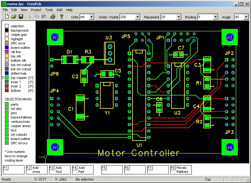
Step 3: Transition to PCB Layout
Once your schematic is ready, it’s time to create the physical layout of your board. This is where beginner PCB layout skills come into play. Switch to the PCB editor in your software. The components from your schematic will appear, ready to be placed on the board.
Follow these steps for a simple PCB layout:
- Set Board Dimensions: Define the size of your PCB. For a small project, a 5cm x 5cm board might be enough. Keep it compact but leave room for components.
- Place Components: Drag components onto the board. Group related parts together (e.g., place a decoupling capacitor near an IC to reduce noise—typically a 0.1μF capacitor for a 5V circuit).
- Arrange for Efficiency: Position components to minimize the length of traces (wires on the PCB). Shorter traces reduce resistance and interference. For example, keep high-current paths under 1cm if possible.
- Stick to Single-Layer (if Beginner-Friendly): For single-layer PCB design, place all traces on one side of the board. This keeps things simple and often cheaper to manufacture.
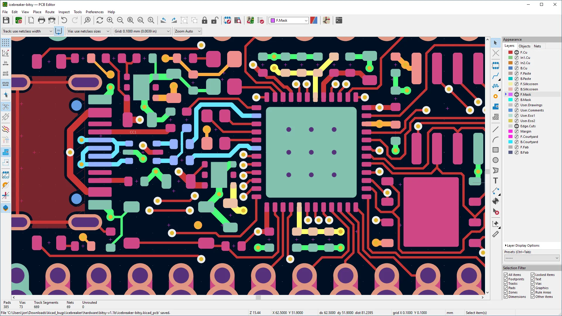
Step 4: Route Your Traces
Routing is the process of drawing the copper paths (traces) that connect your components on the PCB. This step can make or break your design, so take your time.
- Trace Width: Use wider traces for power lines (e.g., 0.5mm or 20 mil for 1A of current) to handle higher currents without overheating. Signal traces can be narrower (e.g., 0.25mm or 10 mil).
- Avoid Sharp Angles: Route traces at 45-degree angles instead of 90-degree turns to reduce signal reflection in high-speed designs (above 1MHz).
- Keep Traces Short: Minimize trace length to reduce resistance (e.g., a 10cm trace of 10 mil width might have 0.05Ω resistance, which can impact low-voltage signals).
- Ground Plane: If possible, create a ground plane (a large copper area connected to ground) on your board to reduce noise and improve stability.
Most easy PCB software includes an auto-routing feature, but for your first design, try manual routing to understand the process better. Run the DRC again to ensure there are no overlaps or errors.
Step 5: Finalize and Export Your Design
With your layout complete, it’s time to prepare your design for manufacturing. Check for any warnings or errors using the software’s DRC tool. Ensure all components have the correct footprints (physical shapes) and that your board dimensions fit your project’s needs.
Export your design files in a standard format like Gerber, which most manufacturers use. These files include layers for copper traces, silkscreen (text on the board), and drill holes. Many free PCB design software tools make this process straightforward with built-in export options.
Additionally, generate a Bill of Materials (BOM) listing all components and their quantities. This helps when sourcing parts for assembly.
Step 6: Review and Order Your PCB
Before sending your design for production, double-check everything. Open the Gerber files in a viewer (many are available online for free) to ensure they look correct. Look for misplaced traces, missing holes, or incorrect board outlines.
Once you’re confident, submit your files to a trusted manufacturer like ALLPCB for high-quality results. Many manufacturers offer affordable options for small runs, perfect for beginners. A typical cost for a 5cm x 5cm single-layer board might start at just a few dollars for a batch of five.
Tips for Success in Beginner PCB Layout
As you embark on your PCB design tutorial journey, keep these tips in mind for better results:
- Start Small: Begin with a simple PCB layout like an LED circuit or a basic power supply before tackling complex designs.
- Use Tutorials: Many free PCB design software platforms have built-in guides or video walkthroughs. Take advantage of these resources.
- Plan for Assembly: Leave enough space between components (at least 0.5mm) for soldering, especially if you’re doing it by hand.
- Test Incrementally: After receiving your PCB, test it with a multimeter to ensure continuity and correct voltages (e.g., 5V at power pins).
Common Mistakes to Avoid in Single-Layer PCB Design
Even with easy PCB software, beginners can make errors. Here are pitfalls to watch out for:
- Ignoring Trace Width: Thin traces can overheat with high current. Use an online calculator to determine the right width based on current (e.g., 1A needs about 0.5mm at 1oz copper thickness).
- Poor Component Placement: Placing components too close can make soldering difficult or cause heat issues.
- Forgetting Ground Planes: Without a proper ground, noise can interfere with signals, especially in analog circuits.
Conclusion: Bring Your Ideas to Life with ALLPCB
Designing your first PCB is an exciting step in any electronics journey. By following this PCB design tutorial, you’ve learned how to go from a schematic to a simple PCB layout using free PCB design software. Whether you’re focusing on single-layer PCB design or exploring online PCB design tools, the process is within reach for beginners.
With ALLPCB, turning your design into reality is seamless. Our platform supports hobbyists and professionals alike with affordable manufacturing and fast turnaround times. Start small, learn from each project, and soon you’ll be crafting complex boards with confidence. Take the leap today—your first PCB is just a few clicks away!


