 ALLPCB


When designing printed circuit boards (PCBs) for power electronics, a common question arises: are there standard PCB dimensions used in this field? The short answer is that while there are no universally fixed dimensions for PCBs in power electronics, certain guidelines, industry practices, and application-specific requirements often influence the size and layout of these boards. Factors like thermal management, component placement, and power requirements play a significant role in determining dimensions.
In this comprehensive guide, we’ll dive deep into the factors that shape PCB dimensions in power electronics, explore common practices, and provide actionable insights for engineers looking to optimize their designs. Whether you’re working on high-power converters, inverters, or other systems, understanding these principles can help you create efficient and reliable PCBs.
Understanding PCB Dimensions in Power Electronics
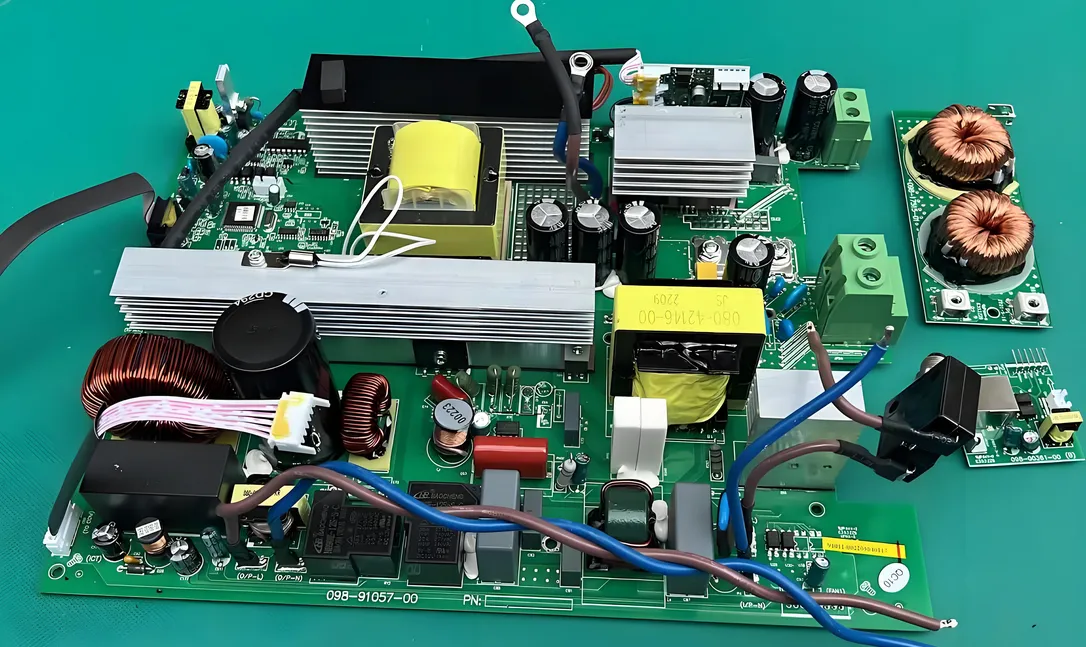
Power electronics involve circuits that handle high voltages and currents, often for applications like power supplies, motor drives, renewable energy systems, and electric vehicles. Unlike standard PCBs used in low-power applications, those in power electronics must accommodate larger components, manage significant heat dissipation, and ensure safety through proper spacing and insulation. As a result, the dimensions of these PCBs are often dictated by practical needs rather than a strict standard.
While organizations like the Institute of Printed Circuits (IPC) provide guidelines such as IPC-2221 for trace widths and spacing, they do not mandate specific board sizes. Instead, dimensions are typically customized based on the application, available enclosure space, and electrical requirements. Let’s break down the key factors that influence PCB dimensions in power electronics.
Factors Influencing PCB Dimensions in Power Electronics
1. Power and Current Requirements
The amount of power a circuit handles directly impacts the size of the PCB. High-power applications require thicker copper traces to carry large currents without overheating. For instance, a trace carrying 10A of current might need a width of 2.5mm or more on a 1oz copper layer, as per IPC-2221 standards. Wider traces and larger components, such as high-power MOSFETs or inductors, necessitate more board space, increasing the overall dimensions.
Additionally, high-current paths often require multiple layers to distribute current evenly and reduce resistance. A 4-layer or 6-layer board might be needed for a 500W power supply, whereas a simple low-power circuit could fit on a single-layer board. This need for additional layers can also affect the board's thickness, typically ranging from 1.6mm to 2.4mm for power applications.
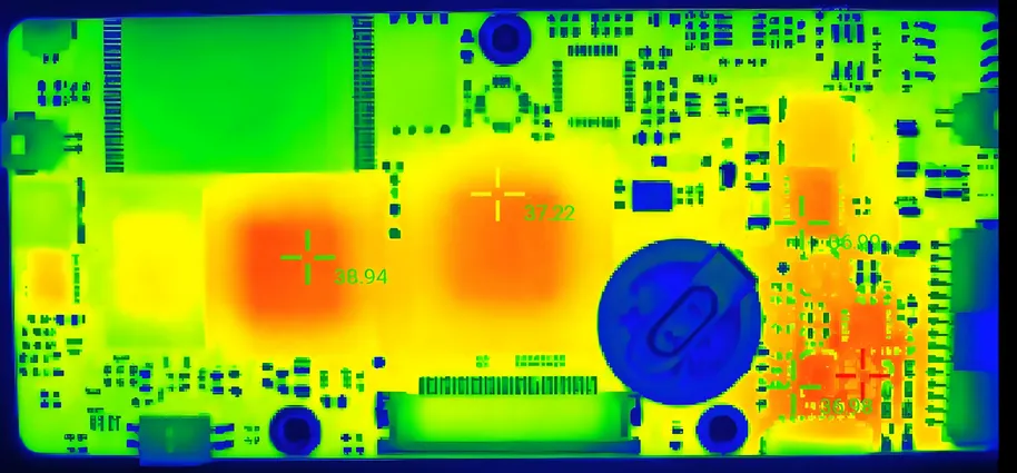
2. Thermal Management Needs
Heat dissipation is a critical concern in power electronics. Components like power transistors and diodes generate significant heat during operation, and the PCB must be designed to manage this heat effectively. Larger board sizes can provide more surface area for heat dissipation, often supplemented by heat sinks or thermal vias.
For example, a PCB for a 100W DC-DC converter might measure 100mm x 80mm to allow space for thermal pads and vias, ensuring heat is transferred away from critical components. In contrast, compact designs may use metal-core PCBs (MCPCBs) to improve thermal conductivity, allowing for smaller dimensions without sacrificing performance.
3. Component Size and Placement
Power electronics often involve bulky components like transformers, capacitors, and inductors, which require substantial board space. A high-voltage capacitor for a 1kW inverter, for instance, might have a footprint of 20mm x 30mm or larger. Arranging these components efficiently while maintaining clearance for safety (e.g., creepage and clearance distances of 3mm or more for 500V applications per IPC standards) often dictates the minimum board size.
Moreover, the layout must minimize parasitic inductance and resistance, which can affect performance at high frequencies. This often means placing power components close to each other, potentially reducing board size, but also ensuring enough space for proper routing and isolation.
4. Enclosure and Mounting Constraints
The physical space available in the final product often sets the maximum dimensions for a PCB. For example, a PCB for an automotive power module might need to fit within a 150mm x 100mm enclosure, while a desktop power supply could accommodate a larger 200mm x 150mm board. Mounting holes, connectors, and other mechanical features also influence the board’s shape and size, sometimes leading to non-rectangular designs.
5. Safety and Regulatory Standards
Safety standards, such as those from the International Electrotechnical Commission (IEC) or Underwriters Laboratories (UL), often require specific spacing between high-voltage and low-voltage areas on a PCB. For instance, a circuit operating at 600V might need a creepage distance of 8mm or more to prevent arcing. These requirements can increase the board’s dimensions to ensure compliance, especially in industrial or medical power electronics.
Common PCB Sizes in Power Electronics Applications
While there are no strict standards for PCB dimensions, certain sizes have become common in power electronics due to practical considerations and industry trends. Below are some typical dimensions for different applications:
- Small Power Supplies (10-50W): Often around 50mm x 50mm to 80mm x 60mm, fitting compact enclosures for consumer electronics like chargers.
- Medium Power Converters (100-500W): Typically 100mm x 80mm to 150mm x 100mm, balancing component space and thermal needs for applications like LED drivers.
- High-Power Inverters (1kW and above): Can range from 200mm x 150mm to 300mm x 200mm or larger, accommodating large components and heat sinks for industrial or renewable energy systems.
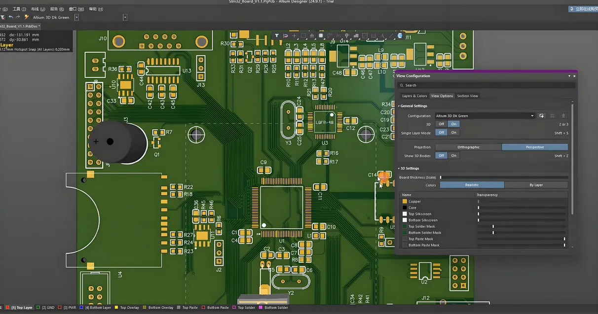
These sizes are not fixed but serve as a starting point. Engineers often adjust dimensions based on specific project needs, using design software to simulate layouts and ensure optimal performance.
Panelization and Manufacturing Considerations
Another factor influencing PCB dimensions in power electronics is panelization during manufacturing. PCBs are often produced in larger panels (e.g., 18” x 24” or 460mm x 610mm) to optimize cost and efficiency. Designing a board with dimensions that fit efficiently into these panels can reduce waste and lower production costs. For instance, a 100mm x 100mm board might be arranged in a 4x5 grid on a panel, maximizing the number of units per sheet.
However, power electronics PCBs sometimes require thicker substrates or special materials like high-Tg FR4 or metal cores, which can limit panel size options. Engineers must balance design needs with manufacturing constraints to achieve cost-effective solutions.
Design Tips for Optimizing PCB Dimensions in Power Electronics
Creating an efficient PCB for power electronics involves careful planning to balance size, performance, and cost. Here are some practical tips to guide your design process:
- Prioritize Thermal Design: Use thermal simulation tools to identify hot spots and ensure adequate spacing for heat dissipation. Consider larger boards or additional layers if heat is a major concern.
- Minimize Trace Lengths: Shorter traces reduce resistance and inductance, improving efficiency. This can sometimes allow for smaller board sizes, provided safety spacing is maintained.
- Use High-Density Layouts: Where possible, opt for surface-mount components over through-hole parts to save space. Ensure proper clearance for high-voltage areas.
- Adhere to Standards: Follow IPC guidelines for trace widths, spacing, and other parameters to avoid redesigns. For example, a 5A trace on a 2oz copper layer might need a width of 1.2mm to prevent overheating.
- Plan for Scalability: If your design might need future upgrades, leave some extra space for additional components or improved cooling solutions.
Challenges in Standardizing PCB Dimensions for Power Electronics
Standardizing PCB dimensions in power electronics is challenging due to the diverse range of applications and requirements. A board for a 5V, 2A USB charger has vastly different needs compared to a 10kW industrial inverter. Additionally, advancements in component technology, such as smaller, more efficient power ICs, continuously change the landscape of PCB design, making fixed dimensions impractical.
Instead of rigid standards, the industry relies on flexible guidelines and best practices. Engineers must adapt to specific project constraints, balancing electrical performance, thermal management, and physical space to determine the optimal dimensions for each design.
How to Choose the Right Dimensions for Your Power Electronics PCB
Selecting the appropriate dimensions for a power electronics PCB starts with a clear understanding of your project’s requirements. Begin by calculating power and current needs to determine trace widths and layer counts. Next, consider thermal management—will a larger board or specialized materials be necessary? Factor in component sizes, enclosure limits, and safety standards to finalize the layout.
Using design software, create multiple iterations of your PCB layout to test different sizes and configurations. Simulate electrical and thermal performance to ensure reliability under operating conditions. Finally, consult with manufacturing partners to confirm that your chosen dimensions align with production capabilities and cost targets.
Conclusion: Flexibility Over Fixed Standards
In power electronics, there are no universal standard PCB dimensions, but practical considerations and industry guidelines shape the size and layout of these boards. Factors like power requirements, thermal management, component placement, and safety standards all play a role in determining the optimal dimensions for a given application. By understanding these influences and following best practices, engineers can design PCBs that deliver reliable performance while meeting project-specific constraints.
At ALLPCB, we’re committed to supporting your power electronics projects with high-quality manufacturing solutions tailored to your unique needs. Whether you’re designing a compact charger or a high-power industrial system, our expertise ensures your PCB meets the highest standards of efficiency and reliability. Start your next project with confidence, knowing that every dimension and detail is optimized for success.


