 ALLPCB


In the fast-evolving world of electronics, designing compact, efficient, and high-performing printed circuit boards (PCBs) is more critical than ever. SMT chokes, or surface mount technology chokes, have emerged as a game-changer in this space. These small yet powerful components help manage electromagnetic interference (EMI) and ensure stable power delivery in high-density PCB layouts. If you're looking to optimize your PCB design for compact electronics, understanding surface mount choke selection, SMT choke footprint, and other key factors like reflow soldering SMT chokes is essential.
In this comprehensive guide, we'll dive deep into how SMT chokes are transforming PCB design. From their role in compact electronics to practical tips for high-density PCB choke placement and automated assembly SMT chokes, we've got you covered. Whether you're an electronics engineer or a hobbyist, this blog will provide actionable insights to elevate your designs.
What Are SMT Chokes and Why Do They Matter?
SMT chokes are small inductors designed for surface mount technology, meaning they can be directly mounted onto the surface of a PCB without the need for through-hole connections. These components are primarily used to filter out high-frequency noise in power lines, ensuring clean and stable power delivery to sensitive electronic components. Their compact size and compatibility with automated assembly make them ideal for modern electronics, where space is often at a premium.
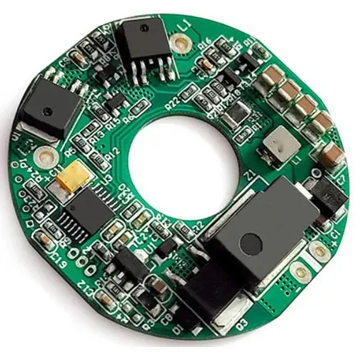
In compact electronics like smartphones, wearables, and IoT devices, every millimeter of PCB space counts. Traditional through-hole chokes are bulkier and require more room, making them less suitable for miniaturized designs. SMT chokes, on the other hand, offer a smaller SMT choke footprint, enabling designers to pack more functionality into tight spaces. Additionally, their ability to handle high currents and frequencies—often ranging from a few microhenries (μH) to several millihenries (mH) in SMT choke inductance values—makes them versatile for various applications.
The Role of SMT Chokes in Compact Electronics
As electronics continue to shrink in size, the demand for components that support miniaturization without sacrificing performance grows. SMT chokes play a vital role in this trend by providing effective noise suppression in a small package. They are commonly used in DC-DC converters, power supplies, and signal lines to prevent EMI from disrupting sensitive circuits.
For instance, in a typical smartphone PCB, multiple SMT chokes might be used to filter noise from the power supply to the processor, ensuring smooth operation even at high frequencies (often above 1 MHz). Their ability to maintain signal integrity in such dense layouts is why SMT chokes are a go-to choice for engineers working on compact, high-performance devices.
Key Factors in Surface Mount Choke Selection
Choosing the right SMT choke for your PCB design is critical to achieving optimal performance. Here are the main considerations for surface mount choke selection:
- Inductance Value: The inductance, measured in microhenries (μH) or millihenries (mH), determines the choke's ability to filter specific frequencies. For example, a 10 μH choke might be suitable for low-frequency noise suppression, while a 1 μH choke could target higher frequencies in switching power supplies.
- Current Rating: Ensure the choke can handle the maximum current in your circuit without saturating. A choke rated for 2 A might work for a small IoT device, but a 5 A rating could be necessary for power-intensive applications.
- DC Resistance (DCR): Lower DCR values (e.g., 0.05 ohms) minimize power loss, which is crucial for battery-powered devices.
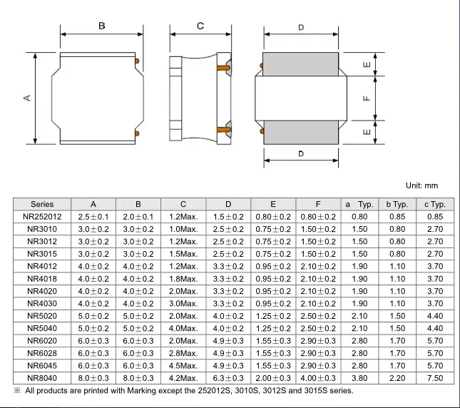
- Size and Footprint: The SMT choke footprint must match the available PCB space. Common sizes include 0603, 0805, or larger 1210 packages, with dimensions as small as 1.6 mm x 0.8 mm for ultra-compact designs.
- Temperature Range: Ensure the choke operates reliably within your device's temperature range, often between -40°C to 125°C for industrial applications.
By carefully evaluating these parameters, you can select an SMT choke that balances performance, size, and cost for your specific application.
Optimizing SMT Choke Footprint for High-Density Designs
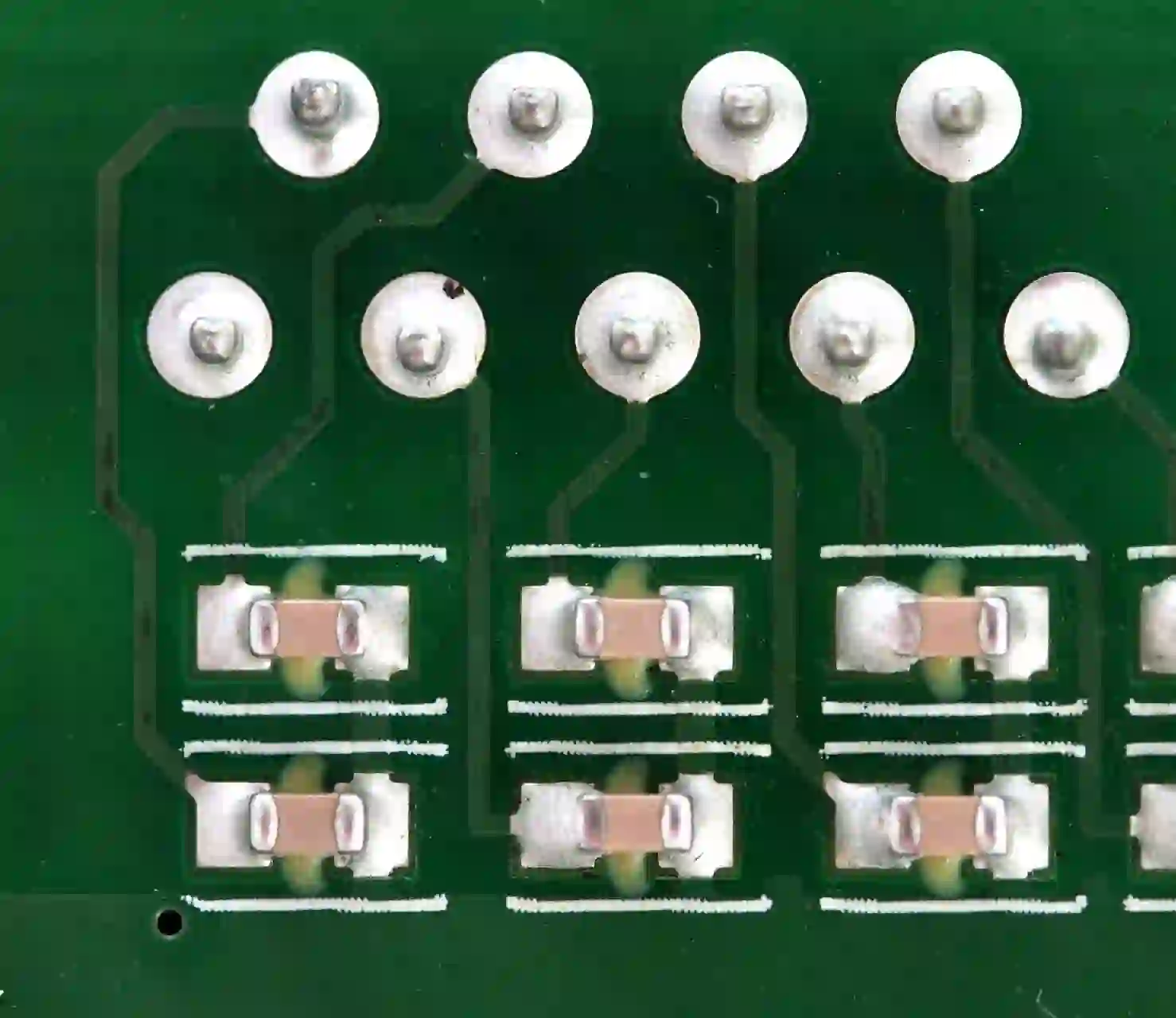
In high-density PCB layouts, every component's placement and footprint matter. The SMT choke footprint directly impacts how much space is available for other components. Smaller footprints, such as those in the 0603 or 0402 package sizes, are ideal for ultra-compact designs, but they often come with trade-offs like lower current ratings or inductance values.
To optimize space, consider the following tips for high-density PCB choke placement:
- Place Chokes Near Power Entry Points: Position SMT chokes close to the power input or switching regulator to suppress noise before it spreads across the board.
- Minimize Trace Lengths: Keep traces between the choke and other components short to reduce parasitic inductance and improve filtering efficiency.
- Avoid Crowding: Even in dense layouts, ensure adequate spacing around the choke to prevent thermal issues or interference with nearby components.
- Use Multi-Layer Boards: For extremely tight designs, utilize inner layers of the PCB for routing, freeing up surface space for SMT chokes and other components.
By strategically planning the placement and footprint of SMT chokes, you can maximize the efficiency of your high-density PCB design without compromising performance.
Reflow Soldering SMT Chokes: Best Practices
One of the advantages of SMT chokes is their compatibility with automated manufacturing processes, including reflow soldering. Reflow soldering SMT chokes involves melting solder paste to attach the choke to the PCB pads, ensuring a secure and reliable connection. However, improper soldering can lead to issues like tombstoning (where one end of the component lifts off the pad) or insufficient solder joints.
Here are some best practices for reflow soldering SMT chokes:
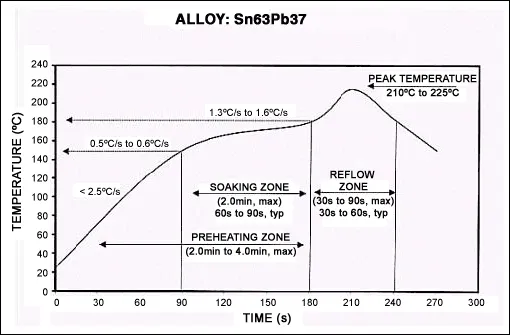
- Use the Correct Solder Paste: Choose a lead-free solder paste with a melting point compatible with the choke's specifications, typically around 217°C to 220°C for SAC305 alloy.
- Optimize Stencil Design: Ensure the stencil aperture matches the choke's pad size to deposit the right amount of solder paste, preventing bridging or insufficient solder.
- Control Reflow Profile: Follow a reflow profile with a gradual ramp-up (1-3°C per second) to the peak temperature, avoiding thermal shock to the choke. A typical peak temperature might range from 240°C to 260°C, held for 20-40 seconds.
- Inspect Post-Soldering: Use automated optical inspection (AOI) to check for soldering defects, ensuring the choke is properly aligned and connected.
By adhering to these guidelines, you can achieve consistent and reliable soldering results for SMT chokes in your PCB assembly process.
Automated Assembly of SMT Chokes: Streamlining Production
Modern electronics manufacturing relies heavily on automation to achieve high throughput and precision. SMT chokes are designed for automated assembly SMT chokes, making them compatible with pick-and-place machines and high-speed production lines. This compatibility reduces manual labor, lowers costs, and minimizes human error.
To ensure smooth automated assembly of SMT chokes, consider these tips:
- Standardize Component Packaging: Use tape-and-reel packaging for SMT chokes to facilitate seamless loading into pick-and-place machines.
- Accurate Footprint Libraries: Maintain up-to-date PCB design libraries with precise SMT choke footprints to avoid placement errors during assembly.
- Optimize Machine Settings: Calibrate pick-and-place machines to handle the specific size and weight of SMT chokes, ensuring accurate placement on pads as small as 0.4 mm x 0.2 mm for tiny components.
- Integrate Quality Checks: Incorporate in-line inspection systems to detect misaligned or missing chokes during the assembly process.
Automation not only speeds up production but also ensures consistent quality, which is crucial for high-volume manufacturing of compact electronics.
Understanding SMT Choke Inductance Values for Your Design
The inductance value of an SMT choke is one of the most critical parameters in determining its performance. SMT choke inductance values typically range from 0.1 μH to 100 mH, depending on the application. Selecting the right inductance value ensures effective noise filtering and power stability in your circuit.
For example:
- Low Inductance (0.1 μH to 1 μH): Suitable for high-frequency applications like RF circuits or fast-switching power supplies, where minimal inductance is needed to filter out noise above 10 MHz.
- Medium Inductance (1 μH to 10 μH): Commonly used in DC-DC converters for smartphones or laptops to smooth out ripple currents at frequencies between 100 kHz and 1 MHz.
- High Inductance (10 μH to 100 mH): Ideal for low-frequency noise suppression in power lines or audio circuits, ensuring stable voltage delivery.
Always refer to the choke's datasheet for detailed specifications, as factors like current rating and saturation behavior can affect performance at specific inductance levels. Simulation tools can also help model how different SMT choke inductance values impact your circuit before finalizing your design.
Challenges and Solutions in Using SMT Chokes
While SMT chokes offer numerous benefits, they come with challenges that designers must address:
- Thermal Management: High-density designs can lead to heat buildup around SMT chokes. Solution: Use chokes with higher temperature ratings and incorporate thermal vias or heat sinks in the PCB layout.
- Saturation Risk: At high currents, chokes can saturate, losing their filtering ability. Solution: Select chokes with a current rating at least 20-30% above your maximum expected current.
- Component Sourcing: Availability of specific SMT chokes can vary. Solution: Work with reliable suppliers and maintain alternative part numbers in your design library.
By anticipating these challenges and implementing the suggested solutions, you can ensure the reliability and performance of your PCB design.
Future Trends: SMT Chokes in Next-Gen Electronics
As electronics continue to evolve, SMT chokes are expected to play an even larger role in next-generation devices. Emerging trends include:
- Smaller Footprints: Advances in manufacturing are leading to even smaller SMT choke footprints, enabling ultra-miniaturized designs for wearables and medical implants.
- Higher Frequency Support: With the rise of 5G and high-speed data applications, SMT chokes are being developed to handle frequencies beyond 100 MHz.
- Integration with Smart Manufacturing: The integration of AI and IoT in manufacturing processes will further enhance the precision of automated assembly SMT chokes, reducing errors and costs.
Staying ahead of these trends will help engineers design cutting-edge electronics that meet the demands of tomorrow's market.
Conclusion: Elevate Your PCB Design with SMT Chokes
SMT chokes are revolutionizing PCB design by enabling compact, efficient, and high-performing electronics. From careful surface mount choke selection to optimizing high-density PCB choke placement, every aspect of using these components can significantly impact your design's success. By mastering techniques like reflow soldering SMT chokes and leveraging automated assembly SMT chokes, you can streamline production while maintaining quality.
Whether you're working on a small IoT device or a complex industrial system, understanding SMT choke inductance values and footprints will empower you to create innovative solutions. As technology advances, SMT chokes will continue to be a cornerstone of compact electronics, helping engineers push the boundaries of what's possible.
Start integrating SMT chokes into your next PCB design and experience the difference they can make in achieving miniaturization without compromise. With the right knowledge and tools, your designs can reach new heights of performance and efficiency.


