 ALLPCB


If you're diving into DIY stencil printing for electronics assembly, you're likely looking for a reliable way to apply solder paste for PCB assembly. This guide will walk you through the essentials of stencil printing for SMT (Surface-Mount Technology) projects, offering practical tips and tricks to ensure successful results. Whether you're a hobbyist or a small-scale manufacturer, mastering DIY stencil printing can save time and improve the quality of your builds.
In this blog, we'll cover everything from the basics of stencil printing to advanced techniques for precision and efficiency in electronics assembly. Let's get started with actionable advice to help you succeed in your PCB projects.
What Is DIY Stencil Printing for Electronics Assembly?
DIY stencil printing is a technique used in electronics assembly to apply solder paste onto a printed circuit board (PCB) before placing surface-mount components. A stencil, typically made of stainless steel or a durable plastic like Kapton, features precise cutouts that match the PCB's solder pads. By spreading solder paste over the stencil, you deposit the paste only where it's needed, ensuring accurate placement for SMT components.
This method is essential for achieving consistent results in PCB assembly, especially when working with small components that require precise soldering. Unlike manual soldering, stencil printing streamlines the process, making it ideal for both small batches and larger production runs in a DIY setting.
Why Choose DIY Stencil Printing?
Opting for DIY stencil printing offers several advantages for electronics enthusiasts and small-scale producers:
- Cost-Effective: Creating or purchasing affordable stencils reduces the need for expensive automated equipment.
- Precision: Stencils ensure uniform solder paste application, reducing the risk of bridges or insufficient solder.
- Time-Saving: Applying paste to multiple pads at once is faster than manual methods, especially for complex boards.
- Scalability: Perfect for prototyping or small production runs without investing in industrial machinery.
Getting Started with DIY Stencil Printing: Essential Tools and Materials
Before you begin, gather the necessary tools and materials to set up your DIY stencil printing workspace. Having the right equipment ensures smoother assembly and better results for your electronics projects.
Key Tools and Materials
- Stencil: Choose a stencil made of stainless steel (0.1mm to 0.15mm thickness for most SMT components) or a durable plastic for finer details. Custom stencils can be laser-cut or ordered based on your PCB design files.
- Solder Paste: Use a high-quality, lead-free solder paste suitable for SMT assembly. Check the alloy composition (e.g., SAC305 with 96.5% tin, 3% silver, 0.5% copper) for compatibility with your components.
- Squeegee: A metal or hard plastic squeegee helps spread solder paste evenly across the stencil. Ensure it's wider than your stencil for consistent application.
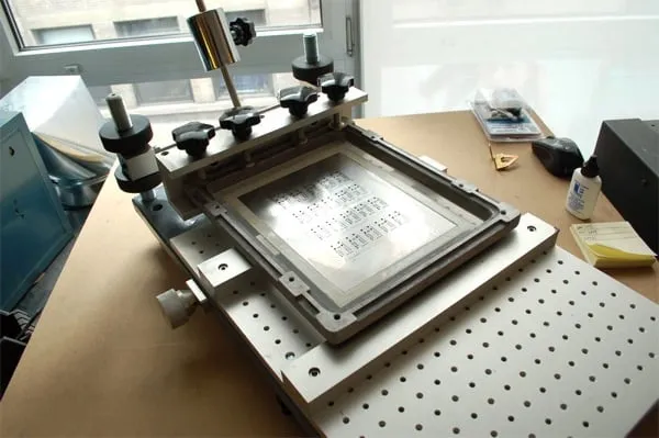
- PCB Holder or Jig: A holder keeps your PCB steady during printing. You can create a simple jig using spare boards or 3D-printed frames for alignment.
- Cleaning Supplies: Isopropyl alcohol (90% or higher), lint-free wipes, and a small brush for cleaning the stencil after use.
- Gloves and Mask: Protect yourself from solder paste, which may contain harmful fluxes or metals.
Step-by-Step Guide to DIY Stencil Printing for PCB Assembly
Follow these steps to achieve precise solder paste application in your electronics assembly projects. Each step is designed to minimize errors and maximize efficiency.
Step 1: Prepare Your Workspace
Set up a clean, well-lit workspace with a flat surface. Dust and debris can contaminate solder paste or interfere with stencil alignment, so wipe down all surfaces and tools with isopropyl alcohol. Wear gloves to avoid skin contact with solder paste and ensure proper ventilation if working with flux-heavy pastes.
Step 2: Align the Stencil with the PCB
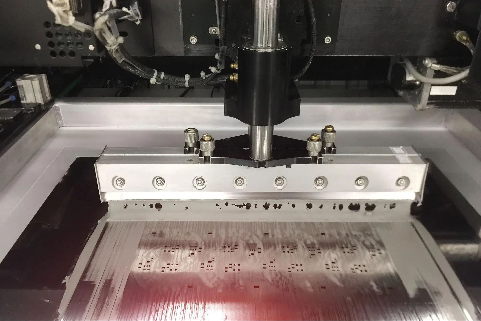
Place your PCB in a holder or jig to keep it secure. Lay the stencil over the PCB, ensuring the cutouts align perfectly with the solder pads. Many stencils include alignment holes or fiducial marks—use these to double-check positioning. If your stencil lacks these features, tape it down lightly to prevent shifting.
Step 3: Apply Solder Paste
Scoop a small amount of solder paste (about 10-20 grams for a standard 10cm x 10cm board) onto one edge of the stencil. Hold the squeegee at a 45-degree angle and drag it across the stencil with steady pressure. This forces the paste through the cutouts onto the PCB pads. Make one or two passes to ensure even coverage, but avoid over-applying, as excess paste can cause solder bridges.
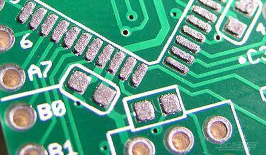
Step 4: Inspect the Paste Application
Carefully lift the stencil straight up to avoid smearing the paste. Inspect the PCB under good lighting or with a magnifying glass. Each pad should have a uniform layer of paste, roughly 0.1mm to 0.15mm thick, depending on component size (e.g., 0.1mm for 0402 resistors, 0.15mm for larger ICs). If you notice gaps or uneven deposits, clean the board and repeat the process.
Step 5: Place Components and Reflow
Using tweezers or a pick-and-place tool, position your SMT components onto the solder paste. Ensure pins align with the pads. Once all components are placed, transfer the PCB to a reflow oven or use a hot air station to melt the solder paste, forming solid connections. Follow the paste manufacturer’s recommended reflow profile (e.g., peak temperature of 245°C for SAC305 alloy).
Tips and Tricks for Successful DIY Stencil Printing
Mastering DIY stencil printing for electronics assembly takes practice, but these tips can help you avoid common pitfalls and improve your results.
1. Choose the Right Stencil Thickness
Stencil thickness directly affects the amount of solder paste deposited. For most SMT components, a thickness of 0.1mm to 0.125mm works well. Thicker stencils (0.15mm or more) are better for larger components with higher solder volume needs, while thinner ones suit fine-pitch ICs to prevent excess paste.
2. Maintain Consistent Squeegee Pressure
Uneven pressure while spreading solder paste can lead to inconsistent deposits. Practice maintaining a steady hand and a 45-degree angle with the squeegee. If you're new to this, start with scrap boards to perfect your technique before working on critical projects.
3. Store Solder Paste Properly
Solder paste is sensitive to temperature and humidity. Store it in a refrigerator at 2-10°C to extend shelf life (typically 6-12 months). Before use, let it warm to room temperature (around 25°C) for 1-2 hours to avoid condensation, which can affect consistency.
4. Clean Your Stencil After Every Use
Residual solder paste on the stencil can clog openings or contaminate future prints. Clean it immediately after use with isopropyl alcohol and a lint-free wipe. For stubborn residue, use a small brush. Dry the stencil completely to prevent rust if it’s metal.
5. Use Alignment Jigs for Repeatability
For multiple boards, create a custom jig or frame to hold both the PCB and stencil in place. This ensures consistent alignment across batches. Some hobbyists design jigs with a 0.1mm clearance around the board outline for easy removal, as shared in online maker communities.
Common Challenges in DIY Stencil Printing and How to Overcome Them
Even with careful preparation, you might encounter issues during DIY stencil printing. Here’s how to tackle some frequent problems in PCB assembly.
Challenge 1: Solder Bridges
Cause: Excess solder paste or misalignment can cause adjacent pads to connect during reflow, creating bridges.
Solution: Use a thinner stencil (e.g., 0.1mm) for fine-pitch components and double-check alignment. After printing, inspect pads and remove excess paste with a fine tip or desoldering braid before reflow.
Challenge 2: Insufficient Solder Paste
Cause: Too little paste or uneven squeegee pressure results in weak solder joints.
Solution: Ensure you apply enough paste at the start (a 2-3mm wide line across the stencil) and maintain consistent pressure. If pads look underfilled, redo the printing process on a cleaned board.
Challenge 3: Stencil Misalignment
Cause: Shifting during printing smears paste or deposits it incorrectly.
Solution: Secure the stencil with tape or a jig. If your design allows, add alignment holes or marks to both the stencil and PCB for precise positioning.
Advanced Techniques for DIY Stencil Printing in Electronics Assembly
Once you’ve mastered the basics, consider these advanced strategies to elevate your SMT assembly process.
Experiment with Stencil Materials
While stainless steel stencils are durable and reusable, plastic stencils (like 0.1mm Kapton) are cheaper and easier to cut at home using a laser cutter or craft knife for simple designs. Test different materials to find what works best for your budget and project scale.
Optimize Reflow Profiles
Different solder pastes require specific reflow profiles for optimal results. For instance, a typical lead-free paste might need a preheat stage at 150-180°C for 60-90 seconds, a soak at 200°C, and a peak at 245°C for 20-30 seconds. Use a controllable reflow oven or monitor temperatures with a thermocouple to avoid thermal shock to components.
Batch Printing for Efficiency
If assembling multiple boards, print solder paste on several PCBs in one session. Lay out identical boards in a grid under a larger stencil or repeat the process with a single-board stencil secured in a jig. This approach minimizes setup time and ensures consistency across units.
Why Stencil Printing Is a Game-Changer for DIY Electronics Projects
DIY stencil printing transforms the way hobbyists and small-scale producers approach electronics assembly. By enabling precise solder paste application, it reduces errors, speeds up production, and delivers professional-quality results without the need for costly equipment. Whether you're prototyping a new design or assembling a small batch of boards, mastering this technique can significantly enhance your workflow.
At ALLPCB, we’re committed to supporting your electronics projects with resources and expertise. While this guide focuses on DIY methods, we also offer professional services to help scale your production when needed. Start with these tips and tricks, and watch your PCB assembly skills reach new heights.
Conclusion: Perfecting Your DIY Stencil Printing Skills
DIY stencil printing for electronics assembly is a powerful skill that can elevate your PCB projects. From selecting the right tools to troubleshooting common issues, this guide has provided a comprehensive roadmap to success. By following the steps and tips outlined, you can achieve consistent, high-quality results in your SMT assembly, whether you're a beginner or an experienced maker.
Practice is key—start small, refine your technique, and experiment with different setups to find what works best for your needs. With patience and attention to detail, you'll master DIY stencil printing and take your electronics assembly to the next level.


