 ALLPCB


Designing a multi-layer PCB can seem daunting, but with the right online resources and tools, it becomes a manageable and even enjoyable process. Whether you're a beginner looking for an easy PCB design solution or a seasoned engineer tackling complex multi-layer boards, this guide will help you navigate the process using free PCB design tools and online PCB design platforms. In this blog, we’ll explore the essentials of multi-layer PCB design, highlight accessible PCB layout software, and provide a step-by-step multi-layer PCB tutorial to simplify your workflow.
What is Multi-Layer PCB Design and Why Does It Matter?
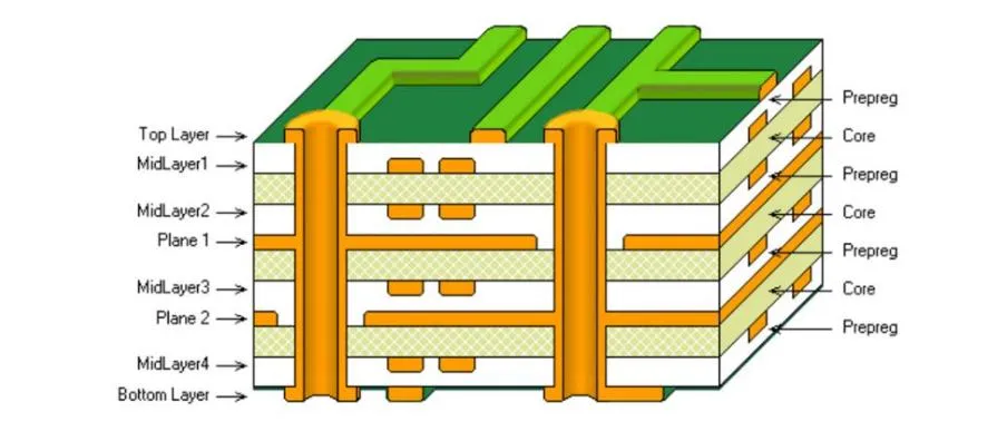
Multi-layer PCBs are circuit boards with more than two layers of conductive material, typically separated by insulating layers. These boards are essential for modern electronics because they allow for higher component density, better signal integrity, and reduced electromagnetic interference (EMI). For instance, a 4-layer PCB might have a top layer for components, a ground plane, a power plane, and a bottom layer for additional routing, optimizing space in devices like smartphones or medical equipment.
The complexity of multi-layer designs often intimidates beginners, but online tools and resources have made it easier than ever to create efficient layouts. By using free PCB design tools and following structured tutorials, you can achieve professional results without breaking the bank.
Benefits of Using Online Resources for Multi-Layer PCB Design
Online resources and tools offer several advantages for PCB designers, especially when working on multi-layer projects. Here are some key benefits:
- Accessibility: Many online PCB design platforms are cloud-based, meaning you can work from anywhere with an internet connection, without needing high-end hardware.
- Cost-Effectiveness: Free PCB design tools provide powerful features at no cost, making them ideal for hobbyists, students, and startups.
- Community Support: Online platforms often come with forums, tutorials, and user communities that share tips and troubleshoot issues, especially for complex multi-layer designs.
- Real-Time Collaboration: Some tools allow multiple users to work on a design simultaneously, which is great for team projects.
These benefits make online tools a go-to choice for simplifying multi-layer PCB design, saving both time and resources.
Top Free PCB Design Tools for Multi-Layer Projects
Choosing the right PCB layout software is critical for a smooth design process. Below are some widely recognized free tools that support multi-layer PCB design. These options are beginner-friendly and equipped with features to handle complex layouts.
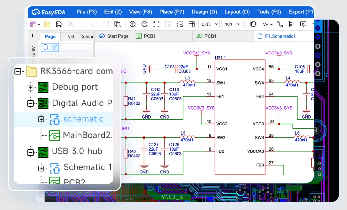
- KiCad: This open-source software is a favorite among engineers for its robust features, including schematic capture, 3D visualization, and support for up to 32 layers. It’s available on Windows, macOS, and Linux, and has a vast library of components.
- CircuitMaker: A free tool designed for hobbyists and open-source hardware designers, it offers multi-layer support and integrates with cloud storage for easy sharing. Its intuitive interface makes it an excellent choice for easy PCB design.
- DesignSpark PCB: This software provides unlimited schematic possibilities and supports multi-layer designs. It’s user-friendly and includes features like design rule checking to avoid errors in your layout.
These free PCB design tools are powerful enough to handle professional multi-layer projects while remaining accessible to beginners. Most of them also offer extensive documentation and tutorials to help you get started.
Step-by-Step Multi-Layer PCB Tutorial for Beginners
Creating a multi-layer PCB may sound complex, but breaking it down into steps makes it manageable. Follow this tutorial using any of the free PCB design tools mentioned above to design a simple 4-layer board for a basic microcontroller circuit.
Step 1: Define Your Project Requirements
Start by outlining the purpose of your PCB. For example, if you’re designing a board for a microcontroller, determine the number of components, power requirements (e.g., 5V or 3.3V), and signal speeds (e.g., up to 100 MHz for high-speed signals). Decide on the number of layers—4 layers are often sufficient for moderate complexity, with a typical stack-up of signal, ground, power, and signal.
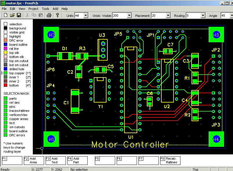
Step 2: Create a Schematic
Use your chosen PCB layout software to draw the schematic. Place components like resistors, capacitors, and your microcontroller, ensuring proper connections. Double-check for errors, as mistakes in the schematic can lead to issues in the layout phase. Most free tools have built-in libraries with common components to speed up this process.
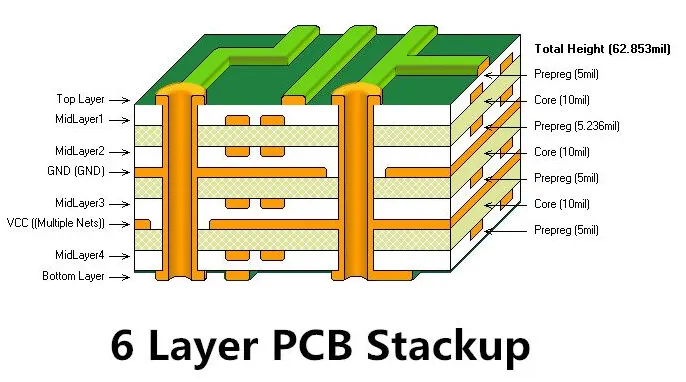
Step 3: Set Up the PCB Stack-Up
In the layout editor, configure your board for multi-layer design. Specify the number of layers (e.g., 4) and assign roles to each layer. For instance, dedicate the second layer as a ground plane to reduce noise and EMI, and the third layer as a power plane for stable voltage distribution. Typical layer thickness might be 1.6mm for the entire board, with copper layers at 1 oz/ft2 for standard current handling.
Step 4: Place Components
Arrange components on the top layer, prioritizing critical parts like the microcontroller near the center for shorter signal paths. Keep high-speed components close to reduce trace lengths, minimizing impedance issues (e.g., aim for trace impedance of 50 ohms for high-speed signals). Use the software’s design rule checker to ensure proper spacing.
Step 5: Route Traces and Vias
Route traces on the top and bottom layers for signals, using inner layers for power and ground. Add vias to connect traces between layers, ensuring minimal via count to reduce manufacturing costs. For example, a signal trace might switch from the top to the bottom layer through a via to avoid crossing other traces. Maintain trace widths based on current needs—use 10 mils for signal traces and 20-30 mils for power traces carrying up to 1A.
Step 6: Add Ground and Power Planes
Create solid copper pours for ground and power planes on the inner layers. A continuous ground plane helps maintain signal integrity by providing a low-impedance return path, reducing noise by up to 20-30% in high-speed designs. Ensure vias connect components to these planes where needed.
Step 7: Run Design Checks
Use the software’s design rule check (DRC) to identify errors like unconnected nets or spacing violations. Fix any issues before finalizing the design. This step is crucial for multi-layer boards, as errors in inner layers are harder to correct after manufacturing.
Step 8: Generate Manufacturing Files
Export Gerber files and a drill file for your PCB. Most free tools support standard formats compatible with manufacturing services. Review the files in a Gerber viewer to ensure all layers align correctly.
This multi-layer PCB tutorial provides a clear roadmap for beginners. With practice, you’ll gain confidence in handling more complex designs using online PCB design platforms.
Tips for Easy PCB Design in Multi-Layer Projects
Multi-layer PCB design doesn’t have to be overwhelming. Here are practical tips to make the process smoother using online tools and resources:
- Start Simple: If you’re new to multi-layer designs, begin with a 4-layer board before moving to 6 or 8 layers. This reduces complexity while you learn.
- Use Design Rules: Set up design rules in your PCB layout software to enforce minimum trace widths (e.g., 6-8 mils for signals) and clearances (e.g., 8 mils) to prevent errors.
- Leverage Tutorials: Many free PCB design tools offer built-in guides or video tutorials. Spend time learning these to understand multi-layer-specific features.
- Optimize Signal Integrity: Route high-speed signals on outer layers and avoid crossing splits in ground planes to maintain impedance, targeting values like 50 ohms for controlled traces.
- Test Virtually: Use simulation features in some tools to check for signal delays or thermal issues before manufacturing. For instance, ensure power traces don’t overheat under a 2A load.
Following these tips will help you achieve an easy PCB design workflow, even for multi-layer boards.
Additional Online Resources for Multi-Layer PCB Design
Beyond free PCB design tools, numerous online resources can enhance your learning and design capabilities. Here are some valuable options:
- Forums and Communities: Platforms like Stack Exchange and Reddit have active electronics communities where users share advice on multi-layer PCB design challenges.
- Video Tutorials: YouTube channels dedicated to electronics often feature step-by-step guides on using PCB layout software for multi-layer projects.
- Online Courses: Websites like Coursera or Udemy offer affordable courses on PCB design, covering topics from basic layouts to advanced multi-layer techniques.
- Design Guides: Many websites publish free guides on PCB stack-up configurations, impedance control, and EMI reduction strategies, often with practical examples.
These resources complement online PCB design tools, providing the knowledge needed to tackle complex projects with confidence.
Common Challenges in Multi-Layer PCB Design and How to Overcome Them
Even with the best tools, multi-layer PCB design comes with challenges. Here’s how to address some common issues:
- Signal Interference: Crosstalk between layers can degrade performance. Mitigate this by maintaining at least 10 mils spacing between high-speed traces and using ground planes to shield signals.
- Thermal Management: High-density designs generate heat. Add thermal vias near power components to dissipate heat, ensuring via diameter is at least 12 mils for effective conduction.
- Manufacturing Constraints: Inner layer errors are costly to fix. Use DRC tools to catch mistakes early and confirm your design meets standard manufacturing tolerances (e.g., minimum drill size of 0.3mm).
- Impedance Mismatch: For high-speed signals, mismatch can cause reflections. Calculate trace width and spacing to match target impedance (e.g., 50 ohms) using online calculators available with many free tools.
By anticipating these challenges and using online resources, you can avoid common pitfalls in multi-layer PCB design.
Why Choose ALLPCB for Your Multi-Layer PCB Manufacturing?
Once your design is ready, partnering with a reliable manufacturing service is crucial. ALLPCB offers comprehensive solutions for multi-layer PCB production, ensuring high-quality results at competitive prices. With support for complex stack-ups, quick turnaround times, and a user-friendly online ordering system, ALLPCB simplifies the transition from design to production. Upload your Gerber files directly to our platform and benefit from instant quotes and expert support to bring your multi-layer PCB to life.
Conclusion
Multi-layer PCB design doesn’t have to be a complicated process. With the wealth of free PCB design tools, online PCB design platforms, and accessible resources available today, anyone can create professional-grade boards. By following a structured multi-layer PCB tutorial, leveraging easy PCB design tips, and using powerful PCB layout software, you’ll streamline your workflow and achieve reliable results. Whether you’re a hobbyist or a professional engineer, these tools and strategies empower you to tackle complex projects with confidence. Start exploring these online resources today and elevate your PCB design skills with ALLPCB as your trusted manufacturing partner.


