 ALLPCB


Printed circuit board (PCB) assembly is a complex process where even the smallest oversight can lead to costly errors. From solder bridges to misaligned components, these issues can disrupt functionality and delay production. PCB rework—the process of correcting these errors after assembly—is a critical skill for engineers aiming to ensure high-quality, reliable boards. In this guide, we'll walk you through the most common PCB assembly errors, proven rework techniques, and best practices to fix them like a pro, saving time and resources.
Whether you're troubleshooting a prototype or refining a high-volume production run, understanding how to address assembly defects efficiently is essential. Let's dive into the common issues and the tools and techniques to resolve them effectively.
Common PCB Assembly Errors
PCB assembly errors often stem from design flaws, manufacturing mishaps, or environmental factors. Below, we outline the most frequent defects engineers encounter, supported by insights from industry experts.
Solder Bridges
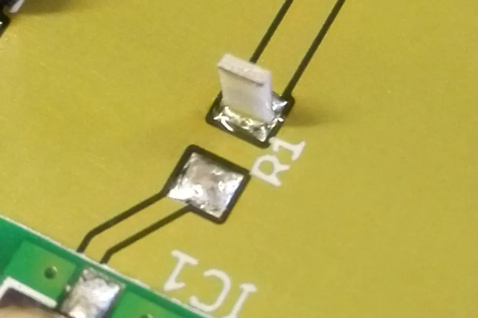
Solder bridges occur when excess solder unintentionally connects two or more conductive features, creating short circuits. This defect is common in densely packed boards with fine-pitch components, where solder paste can smear during reflow. According to industry data, solder bridges account for approximately 15% of PCB assembly defects in high-density designs.
Example: On a 0.5mm pitch QFN package, improper stencil design can deposit excess solder, bridging adjacent pins and causing a short.
Tombstoning
Tombstoning happens when one side of a surface-mount component lifts during reflow, resembling a tombstone. This defect, affecting roughly 10% of prototype assemblies, often results from uneven heating or mismatched pad sizes. For instance, a 0603 resistor may tombstone if one pad reflows faster due to a larger copper plane.
Component Misalignment
Misaligned components occur when parts shift during placement or reflow, leading to poor electrical connections. This issue is prevalent in automated pick-and-place processes, especially with small components like 0402 passives. Studies indicate that misalignment contributes to 20% of rework cases in high-speed production lines.
Insufficient Solder Joints
Insufficient solder joints, where too little solder is applied, result in weak mechanical and electrical connections. This defect is common in boards with improper stencil apertures, affecting up to 12% of assemblies in low-volume runs. For example, a BGA component may fail if solder paste volume is below 0.1mm³ per ball.
Warpage
PCB warpage occurs when the board or components deform due to thermal stress or uneven material expansion. Warpage can misalign components or crack solder joints, particularly in large boards (e.g., 300mm x 200mm) with thin substrates (0.8mm or less). Industry reports suggest warpage affects 5-8% of multilayer boards during assembly.
Tools for Effective PCB Rework
Successful PCB rework requires precision tools to address defects without causing further damage. Here's a rundown of essential equipment and their applications.
Hot Air Rework Stations
Hot air rework stations are ideal for surface-mount technology (SMT) components, allowing controlled heating to desolder or resolder parts. For example, a station with a 0.3mm nozzle can target a single 0402 component without affecting nearby parts. Use adjustable temperature settings (typically 250-350°C for lead-free solder) to prevent thermal damage.
Soldering Irons with Fine Tips
A soldering iron with a 0.5mm or smaller tip is crucial for precise work, such as removing solder bridges or reworking through-hole components. Temperature-controlled irons (set to 300-320°C for lead-free solder) ensure consistent results. For instance, a fine-tip iron can clean excess solder from a 0.4mm pitch QFP pin.
Microscopes and Magnification Tools
Microscopes with 10x-40x magnification are essential for inspecting small components and solder joints. They help identify defects like micro-cracks in BGA solder balls, which are invisible to the naked eye. A digital microscope with a 5MP camera can also document rework for quality control.
Desoldering Braid and Flux
Desoldering braid (e.g., 1.5mm width) removes excess solder from bridges or joints. Paired with no-clean flux, it ensures clean surfaces for resoldering. For example, applying flux to a solder bridge on a 0.5mm pitch connector enhances braid efficiency, reducing rework time by 30%.
PCB Holders
PCB holders secure boards during rework, preventing movement that could damage delicate traces. Adjustable holders accommodate boards from 50mm x 50mm to 400mm x 300mm, ensuring stability during hot air or soldering tasks.
Step-by-Step Rework Techniques
Reworking a PCB requires a systematic approach to avoid introducing new errors. Follow these steps to address common defects effectively.
Step 1: Inspect and Diagnose
Before starting rework, inspect the board using a microscope or automated optical inspection (AOI) system. Identify defects like solder bridges or tombstoned components. For hidden issues, such as BGA solder joint cracks, use X-ray inspection to examine connections under the component.
Example: An X-ray image of a 1.0mm pitch BGA may reveal voids in 10% of solder balls, indicating insufficient reflow.
Step 2: Prepare the Work Area
Set up a clean, well-ventilated workspace with electrostatic discharge (ESD) protection. Use a PCB holder to secure the board and ensure all tools are calibrated. For hot air stations, select a nozzle size matching the component (e.g., 2mm for a 0402 chip, 10mm for a QFP).
Step 3: Remove Defective Components
For SMT components, apply hot air at 300-350°C to melt solder, then gently lift the component with tweezers. For through-hole parts, use a desoldering pump or braid to remove solder. Avoid excessive heat (over 400°C), which can damage pads or traces.
Example: To remove a tombstoned 0603 resistor, heat the component for 10-15 seconds with a 2mm nozzle, then lift it off.
Step 4: Clean and Prep the Board
Clean the rework area with isopropyl alcohol (99% purity) and a lint-free cloth to remove flux residue. Apply fresh flux to pads and use desoldering braid to clear excess solder. Ensure pads are flat and free of debris for reliable resoldering.
Step 5: Place and Solder New Components
Place the new component using precision tweezers or a pick-and-place tool, ensuring alignment with pads. Apply solder paste (e.g., 0.1mm³ for 0402 components) and reflow using a hot air station or reflow oven. For fine-pitch parts, use a soldering iron to touch up joints.
Step 6: Inspect and Test
After rework, inspect solder joints under a microscope for uniformity and voids. Conduct electrical testing, such as continuity checks, to verify functionality. For critical nets, measure resistance (e.g., <0.1Ω for power lines) to ensure reliability.
Example: A reworked BGA should show consistent solder ball shapes under X-ray, with no voids exceeding 25% of ball diameter.
Best Practices to Minimize Rework
While rework is sometimes unavoidable, proactive measures during design and assembly can reduce its frequency. Here are key strategies to enhance PCB quality.
Follow Design for Manufacturability (DFM) Guidelines
Adhere to DFM rules, such as maintaining 0.2mm clearance between components and 0.1mm trace spacing for 1oz copper. Use simulation tools to verify thermal profiles and signal integrity, reducing risks like warpage or impedance mismatches (e.g., 50Ω for high-speed signals).
Verify Bill of Materials (BOM)
Ensure the BOM specifies correct part numbers and footprints. Obsolete or end-of-life (EOL) components, which affect 5% of prototype designs, can lead to rework if not caught early. Cross-check datasheets to confirm pin configurations.
Incorporate Test Points
Add test points (1mm diameter) for critical nets, such as power and ground, to simplify debugging. For a 100mm x 100mm board, include at least 10 test points to cover 90% of nets, reducing rework time by 20%.
Collaborate with Manufacturers
Engage with fabrication and assembly teams during design to address manufacturability concerns. For example, specifying a solder mask color (e.g., green vs. black) can impact yield due to curing differences, affecting 3-5% of production runs.
Challenges in PCB Rework
Rework isn't without challenges, especially with modern, complex PCBs. Here are common hurdles and how to overcome them.
Delicate Components
SMT components like 01005 passives are fragile and prone to damage. Use low-force tweezers and limit heat exposure to 10-15 seconds per joint. For BGAs, employ preheating (150°C) to reduce thermal stress.
Heat Sensitivity
Prolonged heat can damage pads or substrates. For multilayer boards (e.g., 8 layers), keep rework temperatures below 350°C and use heat shields to protect adjacent components.
Complex Designs
Multi-layer PCBs with dense layouts (e.g., 500 components per 100cm²) complicate rework. Use 3D X-ray inspection to navigate internal traces and ensure precise component placement.
How ALLPCB Supports Flawless PCB Production
At ALLPCB, we understand that minimizing rework starts with high-quality manufacturing. Our advanced PCB assembly services, including quick-turn prototyping and global logistics, help engineers achieve error-free boards from the outset. With state-of-the-art equipment like automated optical inspection (AOI) and X-ray systems, we catch defects early, reducing rework by up to 30%. Our DFM analysis ensures designs are optimized for manufacturability, while our 24/7 support connects you with experts to resolve issues fast, keeping your projects on track.
Conclusion
PCB rework is a vital skill for engineers, enabling the correction of assembly errors like solder bridges, tombstoning, and warpage without scrapping boards. By mastering rework techniques—using tools like hot air stations and microscopes—and following DFM best practices, you can achieve professional results that enhance board reliability. Proactive collaboration with manufacturers and thorough testing further minimize rework needs, saving time and costs.
Ready to tackle PCB rework like a pro? Start by inspecting your boards meticulously, choosing the right tools, and partnering with a reliable manufacturer to streamline your process. With these strategies, you'll turn assembly challenges into opportunities for success.


