 ALLPCB


In the world of PCB assembly, achieving precision in solder paste application is critical for ensuring reliable electrical connections and high-quality products. At the heart of this process lies stencil design—a key factor that directly impacts the accuracy and consistency of solder paste deposition. Whether you're an engineer or a manufacturer, mastering stencil design can elevate your surface mount technology (SMT) processes. In this comprehensive guide, we’ll dive deep into the essential elements of stencil design, including stencil thickness, aperture design, area ratio, aspect ratio, fiducial marks, stencil material, and step stencil techniques, to help you achieve flawless results.
Why Stencil Design Matters in Solder Paste Application
Stencil design is the foundation of effective solder paste application in PCB manufacturing. A well-designed stencil ensures the right amount of solder paste is deposited onto the PCB pads, creating strong and consistent solder joints between components and the board. Poor stencil design, on the other hand, can lead to issues like insufficient paste, bridging, or uneven deposits, which result in defective assemblies and costly rework. By focusing on key design parameters, you can optimize your stencil for precision and efficiency, reducing errors and improving overall production quality.
Let’s explore the critical aspects of stencil design that every PCB professional should understand to achieve accurate solder paste application.
1. Stencil Thickness: Finding the Right Balance
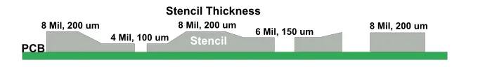
Stencil thickness plays a pivotal role in determining how much solder paste is deposited on the PCB. Typically measured in mils (thousandths of an inch) or micrometers, stencil thickness must be carefully selected based on the component types and pad sizes on your board. For standard SMT components, a stencil thickness of 4 to 6 mils (100 to 150 micrometers) is often ideal. However, finer pitch components, such as 0.4mm pitch QFNs or BGAs, may require thinner stencils—around 3 to 4 mils (75 to 100 micrometers)—to prevent excessive paste deposition and potential bridging.
Conversely, larger components or through-hole parts might need thicker stencils, up to 8 mils (200 micrometers), to ensure enough paste for robust solder joints. The key is to match the stencil thickness to the smallest aperture on your design while considering the paste volume needed for larger pads. A mismatch in thickness can lead to inconsistent deposits, affecting the reliability of your assembly.
2. Aperture Design: Precision in Paste Deposition
Aperture design refers to the size and shape of the openings in the stencil through which solder paste is applied to the PCB pads. Properly designed apertures ensure that the correct amount of paste is deposited without causing defects like smearing or insufficient coverage. The aperture size is often slightly smaller than the pad size—typically reduced by 10-20% in width and length—to account for paste spread during printing and to prevent excess paste from causing shorts.
For fine-pitch components, aperture design becomes even more critical. Reducing the aperture size or adjusting its shape (e.g., using rounded corners instead of sharp edges) can help control paste volume and improve release from the stencil. Laser-cut stmechanical polishing is often used to create precise apertures, ensuring clean edges that facilitate better paste transfer.

3. Area Ratio and Aspect Ratio: Key Metrics for Stencil Performance
Two critical metrics in stencil design are the area ratio and aspect ratio, which help determine how well solder paste will release from the stencil apertures during printing.
Area Ratio
The area ratio is the ratio of the aperture’s open area to the area of the aperture walls. It is calculated as the aperture area divided by the product of the aperture perimeter and stencil thickness. A higher area ratio (ideally above 0.66) indicates better paste release, as there is less surface area for the paste to stick to the walls. For smaller apertures, achieving a high area ratio can be challenging, often requiring thinner stencils to maintain good performance.
Aspect Ratio
The aspect ratio is the ratio of the aperture’s smallest dimension (width or length) to the stencil thickness. A minimum aspect ratio of 1.5 is generally recommended to ensure proper paste release. For example, if your stencil is 5 mils thick, the smallest aperture dimension should be at least 7.5 mils. Failing to meet this threshold can result in paste sticking inside the aperture, leading to incomplete deposits on the PCB.
Balancing area ratio and aspect ratio is essential for optimizing stencil performance, especially for boards with a mix of fine-pitch and larger components.
Image Placement Suggestion: Include a diagram here showing the calculation of area ratio and aspect ratio with labeled dimensions. ALT Text: "Diagram explaining area ratio and aspect ratio in stencil design."
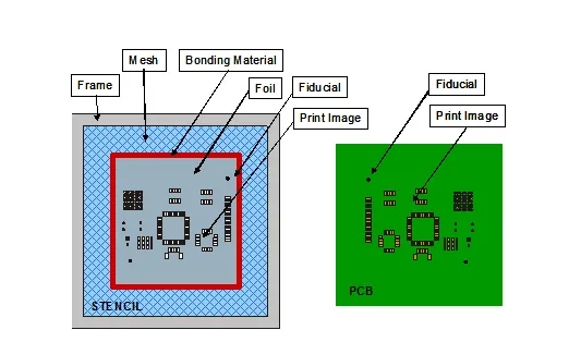
4. Fiducial Marks: Ensuring Alignment Accuracy
Fiducial marks are small reference points on the PCB and stencil that help align the stencil precisely with the board during the solder paste printing process. These marks are typically circular or cross-shaped and are placed in at least two, preferably three, locations on the board and stencil for maximum accuracy. Proper alignment is crucial, especially for high-density boards with fine-pitch components, where even a slight misalignment can cause paste to be deposited off the pads, leading to soldering defects.
When designing fiducial marks, ensure they are clear of solder mask and other obstructions to allow vision systems in automated printers to detect them easily. A fiducial mark diameter of 1mm to 3mm is standard, with a surrounding clearance area at least twice the mark’s diameter to avoid interference.
5. Stencil Material: Durability and Precision
The choice of stencil material significantly affects its durability, precision, and cost. Most stencils today are made from stainless steel due to its strength, resistance to wear, and compatibility with laser-cutting processes. Stainless steel stencils, often in grades like 304 or 316, provide smooth aperture walls, which improve paste release and reduce the need for frequent cleaning.
For applications requiring extreme precision or where stencils will be reused extensively, nickel-plated or electroformed stencils are an option. These materials offer even smoother walls and tighter tolerances but come at a higher cost. For prototype or low-volume production, less expensive materials like Mylar or polyimide can be used, though they lack the durability of metal stencils and are prone to stretching over time.
Selecting the right stencil material depends on your production volume, budget, and the complexity of your PCB design. For most SMT applications, stainless steel strikes a good balance between performance and cost.
6. Step Stencil: Managing Mixed Component Sizes
In modern PCB designs, it’s common to have a mix of component sizes on a single board, from tiny 0201 passives to larger connectors or power components. A uniform stencil thickness may not provide the optimal paste volume for all components, leading to over- or under-pasting. This is where a step stencil comes into play.
A step stencil features varying thicknesses in different areas of the stencil to control solder paste volume. For instance, thinner sections (e.g., 3 mils) can be used for fine-pitch components to limit paste deposition, while thicker sections (e.g., 6 mils) can accommodate larger components that require more paste. Step stencils are created by chemically etching or mechanically milling specific areas of the stencil to reduce thickness, ensuring precise control over paste application across the board.
While step stencils are more complex and costly to manufacture, they are invaluable for high-mix assemblies, reducing defects and improving first-pass yield.
Best Practices for Stencil Design and Usage
Beyond the core elements of stencil design, following best practices can further enhance the accuracy of solder paste application and extend the life of your stencil:
- Regular Cleaning: Clean the stencil after every 5-10 prints to prevent paste buildup, which can clog apertures and cause inconsistent deposits. Use appropriate solvents and wiping techniques to avoid damaging the stencil.
- Storage: Store stencils flat in a dry, dust-free environment to prevent warping or contamination that could affect print quality.
- Inspection: Routinely inspect stencils for wear, especially around fine-pitch apertures, as repeated use can cause aperture walls to degrade, impacting paste release.
- Printer Settings: Optimize printer parameters such as squeegee pressure (typically 0.3-0.5 kg/cm of blade length), print speed (20-40 mm/s), and separation speed to match your stencil design and paste type.
Implementing these practices ensures consistent performance and minimizes downtime in your SMT line.
Conclusion: Elevate Your PCB Assembly with Expert Stencil Design
Mastering stencil design is a game-changer for achieving accurate solder paste application in PCB manufacturing. By carefully considering factors like stencil thickness, aperture design, area ratio, aspect ratio, fiducial marks, stencil material, and the use of step stencils, you can optimize paste deposition for any board layout, from simple designs to complex, high-density assemblies. A well-designed stencil not only improves solder joint quality but also boosts production efficiency by reducing defects and rework.


