 ALLPCB


In high-volume Surface Mount Technology (SMT) assembly, stencil design plays a critical role in ensuring consistent solder paste application and reliable PCB assembly. Whether you're focusing on SMT stencil design, stencil thickness, aperture design, solder paste release, or area ratio, following best practices can significantly improve production efficiency and product quality. This guide dives deep into the essential strategies for optimizing stencil design to meet the demands of high-volume manufacturing.
At its core, effective stencil design ensures precise solder paste deposition on PCB pads, which is vital for forming strong electrical and mechanical connections between components and the board. In this blog, we’ll explore the key factors that influence stencil performance and provide actionable tips to help engineers and manufacturers achieve superior results in SMT assembly.
Why Stencil Design Matters in High-Volume SMT Assembly
In high-volume SMT assembly, even minor issues with stencil design can lead to significant defects, such as insufficient solder paste, bridging, or tombstoning. These defects not only increase rework costs but also delay production schedules. A well-designed stencil ensures uniform paste deposition, minimizes waste, and supports high-speed automated assembly processes.
The primary goal of SMT stencil design is to balance the amount of solder paste applied with the requirements of various component sizes and pad geometries on the PCB. Factors like stencil thickness and aperture design directly impact solder paste release, while the area ratio determines how effectively paste transfers from the stencil to the board. Let’s break down these elements and explore best practices for each.
Choosing the Right Stencil Thickness for Optimal Results
Stencil thickness is one of the most critical parameters in SMT stencil design. It directly affects the volume of solder paste deposited on the PCB pads. For high-volume assembly, selecting the appropriate thickness ensures consistent paste application across thousands of boards.
Typical stencil thicknesses range from 0.1 mm (4 mils) to 0.15 mm (6 mils), depending on the component types and pad sizes on the PCB. Thinner stencils, such as 0.1 mm, are ideal for fine-pitch components like 0.4 mm pitch QFNs or 0201 chip components, as they deposit less paste to prevent bridging. Thicker stencils, like 0.15 mm, are better suited for larger components, such as connectors or power devices, which require more paste for robust solder joints.
However, stencil thickness must be balanced with the area ratio (discussed later) to ensure proper solder paste release. If the stencil is too thick relative to the aperture size, the paste may stick to the stencil walls instead of transferring to the pad. A general guideline is to aim for a stencil thickness that supports an area ratio of at least 0.66 for reliable paste release.
Best Practice: Conduct test runs with different stencil thicknesses during the design phase to identify the optimal value for your specific PCB layout. For mixed-technology boards with both fine-pitch and large components, consider using stepped stencils, which have varying thicknesses in different areas to accommodate diverse paste volume needs.
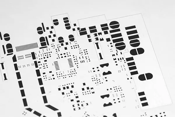
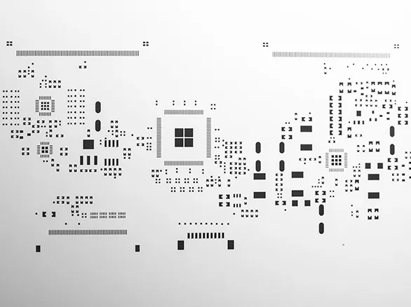
Optimizing Aperture Design for Precision and Consistency
Aperture design refers to the size, shape, and layout of the openings in the stencil through which solder paste is deposited onto the PCB pads. In high-volume SMT assembly, poor aperture design can lead to uneven paste distribution, resulting in defects like insufficient solder or shorts.
For most SMT applications, apertures are designed to be slightly smaller than the PCB pad size—typically 10-20% reduction in area—to prevent excessive paste and reduce the risk of bridging. However, the exact reduction depends on the component type and pad geometry. For example, fine-pitch components may require a 1:1 aperture-to-pad ratio with rounded corners to improve paste release, while larger pads can handle greater reductions.
The shape of the aperture also matters. Rectangular or square apertures are common, but for fine-pitch components, trapezoidal apertures with tapered walls can enhance solder paste release by reducing the contact area between the paste and stencil walls. Additionally, ensure that aperture walls are smooth and free of burrs, as rough edges can trap paste and cause inconsistent deposition.
Best Practice: Use design software to simulate solder paste deposition with different aperture shapes and sizes before manufacturing the stencil. This can help identify potential issues early and save time in high-volume production.
Understanding Area Ratio for Effective Solder Paste Release
The area ratio is a critical metric in stencil design, defined as the ratio of the aperture opening area to the area of the aperture walls. It directly influences solder paste release—the ability of the paste to transfer cleanly from the stencil to the PCB pad without sticking to the stencil.
A higher area ratio indicates better paste release. For reliable performance, industry standards recommend an area ratio of at least 0.66. If the ratio falls below this value, the paste is more likely to adhere to the stencil walls due to surface tension, leading to insufficient solder on the pad. For example, a small aperture (e.g., 0.2 mm x 0.2 mm) in a thick stencil (e.g., 0.15 mm) will have a low area ratio, making paste release challenging.
To calculate the area ratio for a rectangular aperture, use the formula: Area Ratio = (Length x Width) / [2 x (Length + Width) x Thickness]. If the result is below 0.66, consider reducing the stencil thickness or increasing the aperture size where possible.
Best Practice: For high-volume SMT assembly, prioritize stencil designs with area ratios above 0.66, especially for fine-pitch components. If adjustments to thickness or aperture size aren’t feasible, explore advanced stencil technologies like nano-coatings, which reduce paste adhesion to stencil walls and improve release even at lower area ratios.
Material and Manufacturing Considerations for Stencils
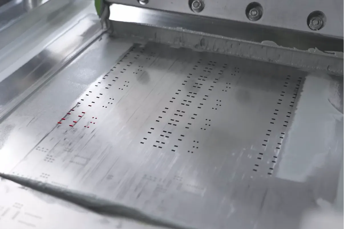
The material and manufacturing process of the stencil also impact its performance in high-volume SMT assembly. Most stencils are made from stainless steel due to its durability and resistance to wear, which is essential for repeated use in large-scale production. High-quality stainless steel stencils maintain their shape and aperture precision even after thousands of print cycles.
Laser-cut stencils are the industry standard for precision, as they produce clean, burr-free apertures with accurate dimensions. For ultra-fine pitch applications (below 0.5 mm), electropolishing or chemical etching can be applied post-cutting to smooth the aperture walls and enhance solder paste release.
Best Practice: Invest in high-quality stainless steel stencils manufactured with laser-cutting technology for consistent results in high-volume production. Regularly inspect stencils for wear or damage, as even small deformations can affect paste deposition and lead to defects.
Advanced Techniques for High-Volume SMT Stencil Design
In high-volume SMT assembly, where efficiency and defect reduction are paramount, advanced stencil technologies can provide a competitive edge. Here are a few techniques to consider:
- Stepped Stencils: As mentioned earlier, stepped stencils have varying thicknesses to accommodate different paste volume requirements on the same board. This is particularly useful for mixed-technology PCBs with both fine-pitch and large components.
- Nano-Coatings: Applying a nano-coating to the stencil surface reduces paste adhesion, improving release even for small apertures with low area ratios. This can extend stencil life and reduce cleaning frequency.
- Multi-Level Stencils: For complex designs, multi-level stencils can be used to deposit different paste volumes in specific areas, ensuring optimal soldering for every component type.
Best Practice: Evaluate the cost-benefit ratio of advanced stencil technologies based on your production volume and defect rates. While these solutions may have higher upfront costs, they can save significant time and resources in high-volume environments by reducing rework and improving yield.
Maintaining Stencils for Long-Term Performance
In high-volume SMT assembly, stencil maintenance is just as important as design. Over time, solder paste residue can build up on the stencil, clogging apertures and causing inconsistent deposition. Regular cleaning with appropriate solvents or ultrasonic cleaners helps maintain stencil performance and prevents defects.
Additionally, store stencils in a clean, dry environment to avoid contamination or physical damage. Use protective covers or frames to prevent bending or scratching during handling.
Best Practice: Implement a routine cleaning schedule based on production volume. For example, clean the stencil after every 5,000 prints or at the end of each shift, whichever comes first. Track stencil usage and replace it when signs of wear, such as deformed apertures, are detected.
Testing and Validation in Stencil Design
Before committing to full-scale production, validate your stencil design through testing. Use a small batch of PCBs to evaluate solder paste deposition, inspecting for issues like insufficient paste, bridging, or uneven distribution. Employ tools like solder paste inspection (SPI) systems to measure paste volume and alignment accurately.
Testing also helps fine-tune parameters like stencil thickness and aperture design. If defects are detected, adjust the design and retest until optimal results are achieved. This upfront effort can prevent costly issues during high-volume runs.
Best Practice: Incorporate SPI into your quality control process to monitor stencil performance over time. Use data from these inspections to identify trends and make proactive adjustments to stencil design or maintenance routines.
Conclusion: Mastering Stencil Design for High-Volume SMT Success
Effective SMT stencil design is the foundation of successful high-volume SMT assembly. By carefully considering factors like stencil thickness, aperture design, solder paste release, and area ratio, manufacturers can achieve consistent, high-quality results while minimizing defects and downtime.
Start with the basics—selecting the right thickness and optimizing aperture geometry—then refine your approach with advanced techniques like stepped stencils or nano-coatings as needed. Regular maintenance and thorough testing further ensure that your stencil performs reliably across thousands of production cycles.
By following these best practices, you can streamline your SMT assembly process, improve yield, and deliver top-notch products to your customers. With the right stencil design, high-volume manufacturing becomes not just manageable, but a competitive advantage.


