 ALLPCB


If you're looking to master the art of assembling double-sided PCBs, understanding solder paste stencils is key. These tools are essential for precise solder paste application, ensuring strong connections and high-quality results in PCB assembly. In this comprehensive guide, we'll dive deep into the world of solder paste stencils, focusing on their role in double-sided PCB soldering, SMT stencils, reflow soldering, and effective solder paste application techniques. Whether you're a hobbyist or a professional, this guide will equip you with the knowledge to optimize your PCB assembly process.
What Are Solder Paste Stencils and Why Are They Important?
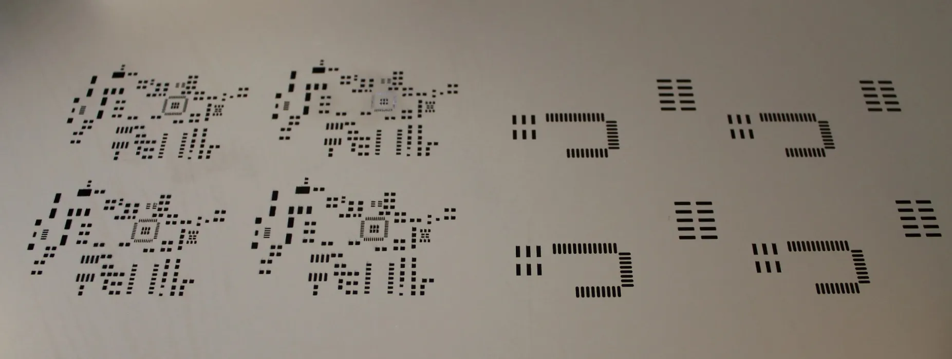
Solder paste stencils are thin sheets, often made of stainless steel, with laser-cut openings that match the layout of a PCB's surface mount components. These stencils allow for accurate and consistent application of solder paste onto the PCB before components are placed and soldered. For double-sided PCBs, where components are mounted on both sides, stencils play a crucial role in ensuring precision and avoiding errors during the soldering process.
The importance of solder paste stencils lies in their ability to streamline the PCB assembly process. Without them, applying solder paste manually would be time-consuming and prone to mistakes, leading to uneven deposits, shorts, or insufficient solder joints. By using stencils, you can achieve repeatable, high-quality results, especially in surface mount technology (SMT) applications.
Understanding Double-Sided PCBs and Their Challenges
Double-sided PCBs have components mounted on both the top and bottom layers, allowing for more compact and complex designs compared to single-sided boards. While this offers greater flexibility, it also introduces unique challenges during assembly, especially when it comes to soldering.
One major challenge is ensuring that components on one side are not disturbed while soldering the other side. This requires careful planning, precise solder paste application, and often the use of adhesives or specific reflow soldering techniques. Solder paste stencils are vital in this process, as they help control the amount and placement of solder paste, reducing the risk of defects like tombstoning or component misalignment.
How Solder Paste Stencils Work in PCB Assembly
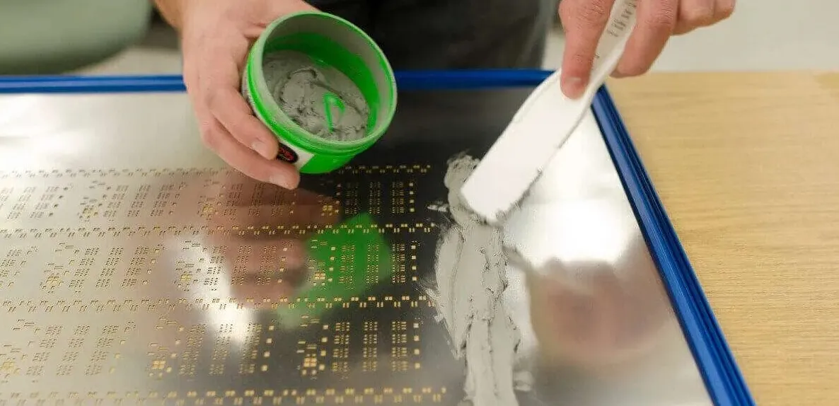
In the PCB assembly process, solder paste stencils act as a template for depositing solder paste onto the board's pads. The stencil is placed over the PCB, and solder paste is spread across it using a squeegee. The paste passes through the stencil's openings and sticks to the pads where components will be placed. Once the stencil is removed, the PCB is ready for component placement and reflow soldering.
For double-sided PCBs, this process is typically done in two stages. First, solder paste is applied to one side, components are placed, and the board undergoes reflow soldering. Then, the process is repeated for the other side. Some advanced assembly lines use adhesives or special fixtures to hold components in place on the first side during the second reflow, preventing them from falling off due to heat and gravity.
Types of Solder Paste Stencils for SMT Applications
There are several types of SMT stencils, each suited to different needs and assembly processes. Understanding these options can help you choose the right one for your double-sided PCB projects.
- Framed Stencils: These are mounted in a rigid frame, making them ideal for high-volume production. The frame keeps the stencil taut, ensuring consistent results over many uses.
- Frameless Stencils: These are standalone sheets without a frame, often used for prototyping or low-volume runs. They are more affordable but require manual alignment, which can be less precise.
- Step Stencils: These have varying thicknesses to accommodate different component sizes on the same board, allowing for tailored solder paste deposits.
- Nano-Coated Stencils: These feature a special coating to improve paste release, reducing defects and cleaning time, especially for fine-pitch components.
For double-sided PCB soldering, framed stencils are often preferred in professional settings due to their durability and precision, while frameless stencils might suffice for smaller projects or testing.
Key Considerations for Solder Paste Application on Double-Sided PCBs
Applying solder paste correctly is critical for successful double-sided PCB assembly. Here are some essential tips to ensure optimal results:
- Stencil Alignment: Ensure the stencil is perfectly aligned with the PCB to avoid misplaced solder paste. Misalignment can lead to soldering defects like bridges or insufficient joints.
- Paste Consistency: Use fresh solder paste with the correct viscosity. Paste that’s too thick or too thin can cause uneven deposits. Store paste at recommended temperatures (typically 2-10°C) and allow it to reach room temperature before use.
- Squeegee Pressure and Speed: Apply consistent pressure and speed when spreading the paste. Too much pressure can damage the stencil, while too little can result in incomplete coverage. A typical squeegee angle of 45-60 degrees works well for most applications.
- Stencil Thickness: Choose a stencil thickness that matches your component sizes. For fine-pitch components (e.g., 0.4mm pitch), a thinner stencil (around 0.1mm) is ideal, while larger components may require a thicker stencil (0.15-0.2mm).
By paying attention to these factors, you can minimize defects and improve the reliability of your solder joints during reflow soldering.
Reflow Soldering Techniques for Double-Sided PCBs
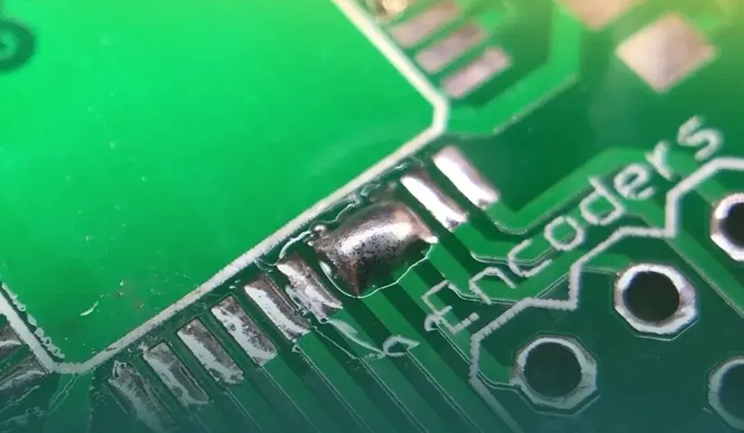
Reflow soldering is the process of heating the PCB to melt the solder paste, creating permanent connections between components and pads. For double-sided PCBs, this process requires extra care to ensure both sides are soldered effectively without damaging components.
Here’s a step-by-step approach to reflow soldering double-sided PCBs:
- First Side Soldering: Apply solder paste to the first side using a stencil, place components, and run the board through a reflow oven. The temperature profile typically includes a preheat phase (150-180°C for 60-90 seconds), a soak phase, and a peak reflow phase (around 220-250°C for 20-40 seconds, depending on the solder paste type).
- Component Securing: For the second side, components on the first side must stay in place during the second reflow. This can be achieved using heat-resistant adhesives (red glue) applied to larger components before the first reflow.
- Second Side Soldering: Flip the board, apply solder paste to the second side with a stencil, place components, and run it through the reflow oven again. Adjust the temperature profile if necessary to prevent overheating components on the first side.
Using a well-calibrated reflow oven with precise temperature control is essential to avoid issues like cold solder joints or thermal damage. Additionally, consider the weight of components on the bottom side during the second reflow, as heavier parts may require extra securing methods.
Common Issues with Solder Paste Stencils and How to Avoid Them
Even with the best tools, issues can arise during solder paste application and reflow soldering. Here are some common problems and solutions:
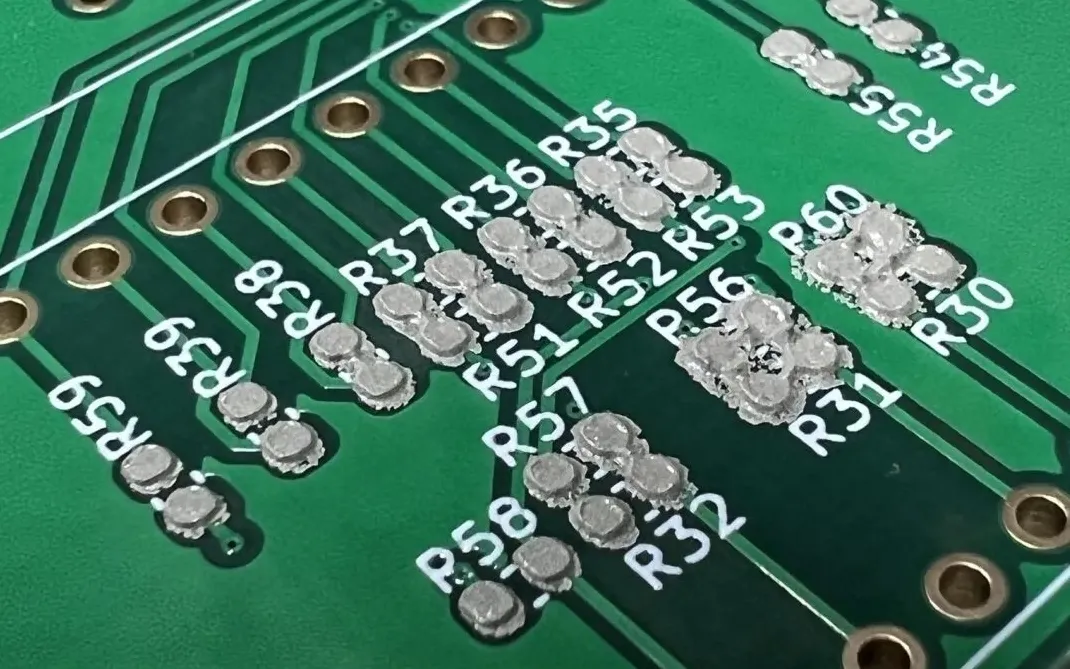
- Solder Bridges: These occur when excess paste connects adjacent pads. Use a thinner stencil or reduce squeegee pressure to control paste volume. Inspect the stencil for wear or damage that might cause leaks.
- Insufficient Solder: If joints are weak, check if the stencil openings are too small or if the paste isn’t being applied evenly. Adjusting stencil design or paste viscosity can help.
- Stencil Clogging: Residue buildup can block stencil apertures, especially with fine-pitch designs. Clean the stencil after every few uses with a suitable solvent and a soft cloth to maintain clear openings.
- Component Misalignment: This often results from poor stencil alignment or uneven paste deposits. Use alignment fiducials on the PCB and stencil for precise positioning.
Regular maintenance of stencils and attention to detail during the assembly process can prevent most of these issues, saving time and resources.
Choosing the Right Solder Paste for Double-Sided PCB Assembly
The type of solder paste you use significantly impacts the quality of your assembly. Solder paste consists of tiny solder particles mixed with flux, and its composition affects melting temperature, wetting properties, and joint strength.
For double-sided PCB soldering, consider these factors when selecting solder paste:
- Lead-Free vs. Leaded: Lead-free solder paste (e.g., SAC305 alloy) is widely used due to environmental regulations. It has a higher melting point (around 217-220°C) compared to leaded paste (around 183°C), so ensure your reflow oven can handle these temperatures.
- Particle Size: Smaller particles (Type 4 or 5, ranging from 15-25 microns) are better for fine-pitch components, while larger particles (Type 3, 25-45 microns) suit standard components.
- Flux Type: No-clean flux is popular for its convenience, as it leaves minimal residue. However, water-soluble flux might be necessary for applications requiring thorough cleaning post-reflow.
Always match the solder paste to your stencil design and component requirements for the best results in SMT assembly.
Best Practices for Stencil Design and Maintenance
A well-designed stencil is the foundation of successful solder paste application. Here are some best practices for stencil design and care:
- Aperture Design: Ensure stencil apertures are slightly smaller than the PCB pads (typically 10-20% reduction) to prevent excess paste and bridging. For fine-pitch components, a 1:1 ratio might be necessary.
- Material and Thickness: Stainless steel stencils with a thickness of 0.1-0.2mm are standard for most applications. Thinner stencils reduce paste volume for smaller components, while thicker ones are better for larger parts.
- Regular Cleaning: Clean stencils after every 5-10 prints to avoid clogging. Use an ultrasonic cleaner or manual wiping with appropriate solvents to remove residue.
- Storage: Store stencils flat in a dry, dust-free environment to prevent warping or damage to the delicate apertures.
Proper design and maintenance extend the life of your stencil and ensure consistent performance during PCB assembly.
Conclusion: Mastering Solder Paste Stencils for Double-Sided PCBs
Solder paste stencils are indispensable tools for achieving precision and efficiency in double-sided PCB soldering. By understanding their role in PCB assembly, selecting the right stencil type, and following best practices for solder paste application and reflow soldering, you can significantly improve the quality of your projects. Whether you're working on a small prototype or a large-scale production run, the tips and techniques shared in this guide will help you navigate the challenges of double-sided PCB assembly with confidence.


