 ALLPCB


If you want to master stencil design for PCB assembly, you've come to the right place. This guide covers everything you need to know to create efficient stencils for surface mount technology (SMT) processes, including stencil printing techniques and aperture design tips. Whether you're new to PCB assembly or an experienced engineer, we'll walk you through the basics of SMT stencils to ensure precision and quality on your projects.
In the following sections, we’ll take a deep dive into stencil design, exploring its importance, key considerations, and best practices. From understanding the basics to optimizing aperture layout for solder paste deposition, this comprehensive resource will provide you with actionable insights to enhance your PCB assembly process.
Why Stencil Design is Important in PCB Assembly
Stencil design is a critical step in PCB assembly, especially for SMT process. A well-designed stencil ensures accurate application of solder paste, which directly affects the quality of component placement and soldering. Poor stencil design can lead to problems such as insufficient solder, bridging or misalignment, resulting in board defects and expensive rework costs.
In SMT assembly, the stencil acts as a template for depositing solder paste onto the PCB pads. The precision of this process determines the adhesion of components during the reflow soldering process. As modern electronic products become increasingly compact, component pitches become smaller and layouts become denser, the tolerance for errors in stencil design becomes lower and lower. A single miscalculation in the size or location of an aperture can lead to significant production delays.
Learn the basics of SMT templates
SMT stencils are thin sheets, usually made of stainless steel, with laser-cut openings, called apertures. These apertures align with the pads of the PCB so that solder paste is applied only where it is needed. Depending on the scale of production, stencils can be framed for automatic printing machines or frameless for manual soldering.
Stencil thickness typically ranges from 0.1 mm to 0.2 mm (4 to 8 mils), depending on component type and pitch. Thinner stencils are ideal for fine-pitch components because they deposit less solder paste, while thicker stencils are better for larger components that require more solder paste. Choosing the right thickness is a trade-off—too thin and you may end up with insufficient solder; too thick and you may end up with bridging between pads.
The materials and manufacturing process are also important. Laser-cut stainless steel stencils are favored for their precision and durability, ensuring consistent results after thousands of prints. Some stencils may also come with a nano-coating to improve solder paste release and reduce cleaning frequency.
Key Factors in PCB Assembly Template Design
Designing a stencil for PCB assembly requires attention to several parameters. Let's break down the most important factors to consider for optimal results.
1. Aperture Design and Sizing
Aperture design is at the heart of stencil functionality. The size and shape of each aperture must match the corresponding pad on the PCB, with slight modifications to account for paste release and component requirements. For most standard components, apertures are designed to be 90-100% of the pad size to prevent excess paste. However, for fine-pitch components (below 0.5 mm), reducing the aperture to 80-90% of the pad size can minimize bridging risks.
The shape of the aperture also plays a role. Rectangular or square apertures are common, but rounded corners can improve paste release by reducing sharp edges where paste might stick. For ball grid arrays (BGAs), circular apertures are often used to match the spherical solder balls, ensuring even deposition.

2. Stencil Thickness
As mentioned earlier, stencil thickness affects the volume of solder paste deposited. A general guideline is to maintain an area ratio (the ratio of aperture opening area to the wall area of the aperture) of at least 0.66 for proper paste release. For example, a 0.15 mm thick stencil with a 0.3 mm wide aperture has an area ratio of 0.5, which may lead to poor paste transfer. Adjusting the thickness or widening the aperture can help achieve better results.
3. Alignment and Fiducial Marks
Accurate alignment between the stencil and PCB is crucial. Fiducial marks—small reference points on the PCB and stencil—help automated printers align the two perfectly. Ensure that your stencil design includes these marks in the same locations as the PCB layout to avoid misalignment during printing.
4. Material and Durability
Stainless steel is the go-to material for most stencils due to its strength and resistance to wear. For high-volume production, investing in a high-quality stencil with a polished finish or nano-coating can extend its lifespan and improve paste release, reducing defects and maintenance costs.
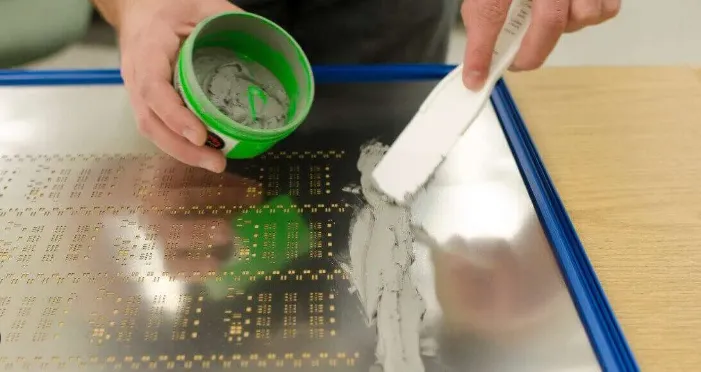
Stencil Printing Techniques for SMT Assembly
Once your stencil is designed, the printing process is the next critical step. Stencil printing involves using a squeegee to push solder paste through the apertures onto the PCB. Here are some techniques and best practices to ensure consistent results.
1. Squeegee Angle and Pressure
The angle of the squeegee, typically set at 45-60 degrees, affects how evenly solder paste fills the apertures. A steeper angle may cause the paste to skip over smaller apertures, while a shallower angle can lead to excess paste buildup. Pressure should be moderate—enough to force paste through the openings but not so much that it damages the stencil or PCB.
2. Print Speed
Print speed should be slow and steady, usually between 20-40 mm per second, to allow the paste to settle properly into the apertures. Faster speeds can result in incomplete filling, especially for fine-pitch components, leading to insufficient solder joints.
3. Paste Selection
Choose a solder paste with the right particle size for your stencil design. For fine-pitch applications, Type 4 or Type 5 paste (particle sizes of 20-38 microns or 15-25 microns, respectively) is recommended to ensure smooth flow through smaller apertures. Larger particle sizes may clog the openings, causing inconsistent deposition.
4. Cleaning and Maintenance
Regular cleaning of the stencil prevents paste buildup, which can block apertures and cause defects. Use a lint-free cloth and a suitable solvent to clean the stencil after every 5-10 prints, or more frequently for high-density designs. Automated printing systems often include under-stencil wiping features to streamline this process.
Optimizing Aperture Design for Precision
Aperture design is often the most challenging aspect of stencil creation, especially for complex boards with mixed component types. Here are some advanced tips to optimize your aperture layouts for better solder paste deposition.
1. Area Ratio and Aspect Ratio
The area ratio, as discussed earlier, should ideally be above 0.66 to ensure proper paste release. Similarly, the aspect ratio (aperture width to stencil thickness) should be at least 1.5. For instance, a 0.2 mm thick stencil should have apertures no narrower than 0.3 mm to avoid paste sticking to the walls.
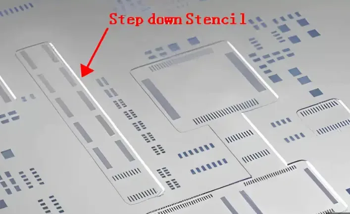
2. Step Stencils for Mixed Components
For boards with both fine-pitch and larger components, consider using a step stencil. This type of stencil has varying thicknesses in different areas—thinner sections for fine-pitch components and thicker sections for larger ones. This approach balances solder paste volume across the board, reducing the risk of defects.
3. BGA and QFN Considerations
For BGAs, reduce aperture size by 10-20% compared to the pad to prevent excess paste, which can cause solder balls to merge. For quad flat no-lead (QFN) packages, a cross-shaped or segmented aperture design can help manage paste volume and prevent voiding under the component.
Common Challenges in Stencil Design and How to Overcome Them
Even with careful planning, stencil design can present challenges. Here are some common issues and solutions to keep your PCB assembly process on track.
1. Solder Bridging
Bridging occurs when excess solder paste connects adjacent pads, often due to oversized apertures or excessive stencil thickness. To fix this, reduce aperture size by 10-15% or use a thinner stencil for fine-pitch areas. Adjusting print pressure and speed can also help.
2. Insufficient Solder Paste
If too little solder paste is deposited, components may not adhere properly during the reflow process. This may be caused by poor solder paste release due to too small aperture size or too low area ratio. Please recalculate the area ratio and consider increasing the aperture size or using a thinner stencil.
3. Misalignment
Stencil misalignment can cause solder paste application to be off-target, resulting in poor component placement. Double-check the fiducial marks and make sure the printer is properly calibrated. For manual printing, use alignment pins or guides to secure the stencil.
Best Practices for Stencil Design in PCB Assembly
To summarize, let’s summarize some best practices that can help you achieve consistent, high-quality results with your SMT templates.
- Collaboration with manufacturers: Work closely with your stencil supplier to ensure the design meets your PCB layout and assembly needs. Provide detailed Gerber files and specifications to ensure accurate production.
- Test and Iterate: Print a small batch of boards to test solder paste deposition and component placement before going into full production. Adjust aperture size or stencil thickness as needed.
- Stay up to date on standards: Follow industry guidelines, such as those from the Institute for Printed Circuits (IPC), to ensure your stencil designs meet quality and performance benchmarks.
- Invest in quality: Choose high-quality materials and manufacturing processes, even if the upfront costs are higher. Durable, accurate formwork reduces defects and rework, saving time and money.
Conclusion: Mastering Stencil Design for Perfect PCB Assembly
Stencil design is the cornerstone of successful PCB assembly, especially in the SMT process where precision is critical. By paying attention to aperture design, stencil thickness, and printing techniques, you can significantly improve the quality of solder paste application and reduce assembly defects. Whether you are dealing with high-density boards or mixed component layouts, the tips and strategies in this guide will help you create an efficient SMT stencil for your needs.
Remember, stencil design is both an art and a science. It requires careful calculation, testing, and collaboration to achieve optimal results. With the right approach, you can streamline the PCB assembly process and ensure reliable, high-performance boards are produced every time. Start applying these principles to your next project and see the difference a well-designed stencil can make.


