 ALLPCB


< there! Are you looking to create custom stencils for your electronics projects? DIY stencil printing is a fantastic way to craft homemade stencils for PCB prototyping and other tasks. In this guide, we'll walk you through the process step-by-step, from understanding the basics to creating your own stencils for precise and professional results in your projects. Now, let’s dive into the detailed world of DIY stencil printing and explore how you can master this skill for your electronics endeavors.
What is DIY Stencil Printing and Why Does It Matter for Electronics Projects?
DIY stencil printing is the process of creating custom stencils at home or in a small workshop to apply patterns, designs, or materials like solder paste onto surfaces such as printed circuit boards (PCBs). For electronics enthusiasts and hobbyists, stencil printing is a game-changer in PCB prototyping. It allows for precise application of solder paste, ensuring accurate component placement and reliable connections in surface-mount technology (SMT) projects.
Using homemade stencils saves time and money compared to outsourcing stencil production. Plus, it gives you full control over the design, letting you tailor stencils to the exact needs of your electronics projects. Whether you're building a small gadget or testing a new circuit design, mastering DIY stencil printing can elevate the quality of your work.
Benefits of Creating Custom Stencils for PCB Prototyping
Custom stencils offer several advantages for electronics projects, especially when working on PCB prototyping. Here are some key benefits:
- Precision: Homemade stencils ensure that solder paste is applied only where it's needed, reducing errors like bridging or insufficient paste. This is critical for SMT components with fine pitch leads, such as 0.5mm or smaller.
- Cost-Effective: Creating your own stencils eliminates the need to purchase expensive pre-made ones, especially for small runs or one-off projects.
- Customization: You can design stencils to match the exact layout of your PCB, accommodating unique pad shapes or non-standard component sizes.
- Speed: With a stencil ready, applying solder paste to multiple boards becomes a quick and repeatable process, ideal for small batch production.
By investing a little time in learning DIY stencil printing, you can achieve professional-grade results without breaking the bank.
Materials and Tools Needed for DIY Stencil Printing
Before you start crafting custom stencils, gather the necessary materials and tools. Here's a comprehensive list to get you started:
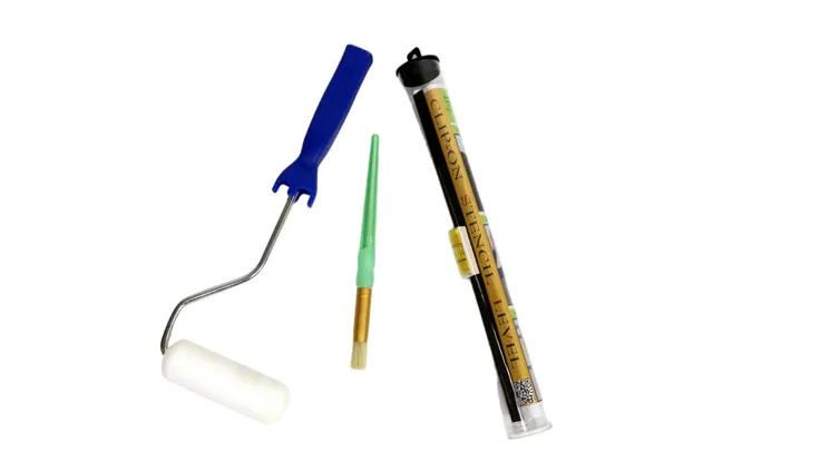
- Stencil Material: Thin plastic sheets (like Mylar or polyester film, 0.1mm to 0.2mm thick), vinyl sheets, or even sturdy paper for temporary stencils.
- Cutting Tools: A craft knife, laser cutter (if available), or vinyl cutter for precise designs.
- Design Software: PCB design software to create or export your stencil layout as a Gerber file or vector image.
- Printer: A standard printer for paper templates or guides if you're cutting by hand.
- Solder Paste: Lead-free or leaded solder paste, depending on your project requirements.
- Squeegee: A small metal or plastic squeegee to spread solder paste evenly through the stencil.
- PCB Boards: Your prototype boards to apply the solder paste onto.
- Masking Tape: To secure the stencil in place during application.
- Cleaning Supplies: Isopropyl alcohol and lint-free cloths to clean the stencil after use.
Having these items on hand will make the process smoother and help you achieve better results in your electronics projects.
Step-by-Step Guide to Creating Homemade Stencils
Now that you have your materials ready, let’s walk through the process of creating custom stencils for your PCB prototyping needs. Follow these steps for a successful outcome.
Step 1: Design Your Stencil Layout
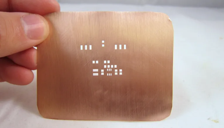
Start by designing the stencil layout using PCB design software. Export the solder paste layer from your PCB design as a Gerber file or convert it into a vector format like SVG. Ensure that the design matches the pad layout of your PCB exactly. Pay attention to the size of openings—typically, they should be slightly smaller than the pad size (about 90% of the pad area) to prevent excess paste.
For fine-pitch components with lead spacing as small as 0.4mm, double-check the design to avoid overly thin stencil walls that could break during cutting.
Step 2: Choose and Prepare Your Stencil Material
Select a material based on durability and cutting method. Mylar sheets (around 0.15mm thick) are a popular choice for laser or vinyl cutting due to their strength and flexibility. If you're cutting by hand, print the design onto paper first as a guide, then transfer it to the stencil material using carbon paper or by taping the printout on top.
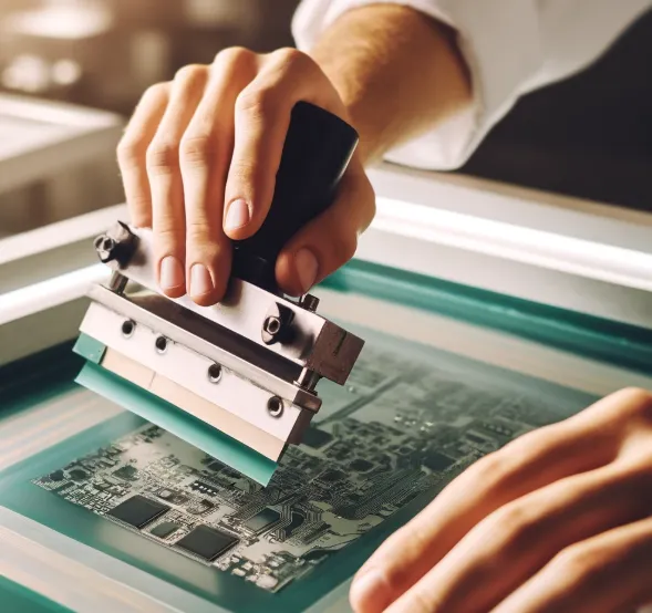
Step 3: Cut the Stencil
If you have access to a laser cutter or vinyl cutter, load the design file and cut the stencil material with precision. Laser cutters can achieve intricate designs with openings as small as 0.2mm, perfect for modern SMT components. For manual cutting, use a sharp craft knife and a steady hand, working on a cutting mat to protect your surface. Take your time to ensure clean, accurate cuts.
Step 4: Test and Refine the Stencil
Place the stencil over a spare PCB or test board to check alignment. Look for any misaligned holes or rough edges that could affect solder paste application. If needed, trim or smooth out the stencil with sandpaper or a small file. Testing early helps avoid issues during the actual application.
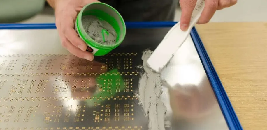
Step 5: Secure the Stencil and Apply Solder Paste
Align the stencil over your PCB and secure it with masking tape to prevent movement. Scoop a small amount of solder paste (about 5-10 grams for a small board) onto the stencil. Using a squeegee at a 45-degree angle, spread the paste across the stencil with even pressure. Ensure all openings are filled without excess paste buildup.
Step 6: Lift the Stencil and Inspect
Carefully lift the stencil straight up to avoid smudging the paste. Inspect the PCB for uniform solder paste deposits. If you notice uneven application, clean the board with isopropyl alcohol, adjust your technique, and try again. Consistency comes with practice.
Step 7: Clean and Store the Stencil
After use, clean the stencil immediately with isopropyl alcohol and a lint-free cloth to remove solder paste residue. Store it flat in a protective sleeve or folder to prevent damage. A well-maintained stencil can be reused multiple times for future projects.
Tips for Successful DIY Stencil Printing
To get the best results from your homemade stencils, keep these practical tips in mind:
- Material Thickness: Use a material thickness of 0.1mm to 0.2mm for most SMT applications. Thicker materials (above 0.25mm) may cause excess paste, while thinner ones can tear easily.
- Paste Consistency: Ensure your solder paste is at room temperature (around 20-25°C) before use. Cold paste can clump, leading to uneven application.
- Practice Pressure: Apply moderate pressure with the squeegee—too much can damage the stencil, while too little leaves gaps in the paste.
- Fine-Pitch Components: For components with lead spacing below 0.5mm, consider reducing stencil openings by 10-15% to prevent bridging during reflow soldering.
- Alignment Marks: Add fiducial marks or alignment holes to your stencil design to ensure perfect positioning on the PCB every time.
These small adjustments can make a big difference in the quality of your PCB prototyping outcomes.
Common Challenges in DIY Stencil Printing and How to Overcome Them
Creating custom stencils for electronics projects isn’t without its hurdles. Here are some common issues and solutions:
- Uneven Solder Paste: This often happens due to inconsistent squeegee pressure or a warped stencil. Use a flat, rigid stencil material and maintain a steady hand during application.
- Stencil Misalignment: If the stencil shifts during use, double-check your securing method. Adding more tape or using a stencil frame can help.
- Clogged Openings: Small holes can clog with dried paste. Clean the stencil after every 2-3 uses, especially for fine-pitch designs.
- Durability Issues: Hand-cut stencils may tear or wear out quickly. Switch to tougher materials like Mylar or limit reuse to avoid degradation.
By anticipating these challenges, you can refine your process and achieve consistent results in your projects.
Advanced Techniques for DIY Stencil Printing
Once you’re comfortable with the basics of DIY stencil printing, explore these advanced methods to take your skills further:
- Laser Cutting for Precision: Investing in or accessing a laser cutter allows for intricate designs with tolerances as tight as 0.1mm, ideal for complex PCBs with high-density components.
- Multi-Layer Stencils: For projects requiring different paste thicknesses, create multi-layer stencils by stacking materials or using step-down designs to control paste volume.
- Reusable Frames: Build a simple frame to hold your stencil taut and aligned over the PCB. This improves repeatability for batch prototyping.
These techniques can help you tackle more ambitious electronics projects with confidence.
Conclusion: Elevate Your Electronics Projects with DIY Stencil Printing
DIY stencil printing is a powerful skill for anyone involved in electronics projects and PCB prototyping. By creating custom stencils, you gain precision, save costs, and unlock endless possibilities for customization in your work. From gathering the right materials to mastering the application process, every step brings you closer to professional-quality results with homemade stencils.
Start small, practice often, and refine your technique as you go. With the tips and steps outlined in this guide, you’re well on your way to making stencil printing a cornerstone of your prototyping toolkit. Dive into your next project with confidence, knowing you can create exactly what you need for success.


