 ALLPCB


Many beginners may be confused about Solder Mask Layer and Paste Mask Layer because they two do have some similarities. In this article, we will introduce the differences between solder masks and paste masks so that beginners can understand better.
Solder Mask
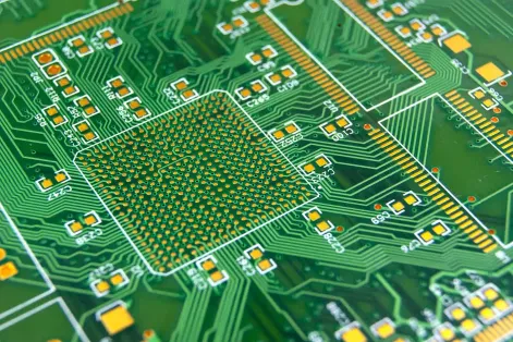
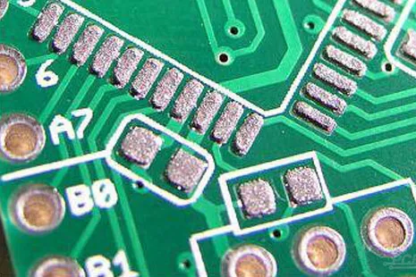
The solder mask is the solder mask layer, except for the pad (surface pads mount pads, plug-in pads, vias) on PCB boards, the other areas should be covered with solder resist ink. These pads are exposed, so as to avoid tin while wave soldering. It is also usually called the solder mask layer or green layer.
The solder mask layer can be divided into Top Layers and Bottom Layers. The small circles or small square circles in the Gerber file are the holes on the solder mask for exposed pads, generally larger than the pad.
Paste Mask
The paste mask layer is generally called PCB stencil in the industry. Generally, the hollow shape size is the same with SMD pads, or slightly smaller. This stencil is used in the SMD automatic assembly soldering process to coat the SMD pads with tin paste. In the surface mount device (SMD) welding process, first, cover the stencil to the circuit board (aligned with the corresponding pads), and then apply the paste, remove the excess paste with a blade, and take away the stencil, so that the solder pads are applied with paste. Afterward, attach components to the solder paste (by hand or assembly machine), and finally through the reflow soldering machine to complete the SMD assembly. Usually, the sizes on the stencil will be smaller than the actual welding pads on the circuit board. The paste mask layer can also divided into Top Paste and Bottom Paste.
Here are some differences between solder mask and paste mask:
1) The openings on the solder mask layer have no solder mask ink, but the openings on the paste mask layer have a paste.
2) The solder mask layer is one part of the circuit board, but the paste mask layer is not. The paste mask layer is just for the stencil.
3) A solder mask is used for applying solder mask ink, but a paste mask is used for applying paste.
4) A solder mask is applied when making a PCB board, but a paste mask is used when assembling.
5) Solder mask has many available colors, but paste mask is usually gray.
Practical Tips for Beginners: Avoiding Common Mistakes in Solder and Paste Masks
When placing pads in your PCB design software, it’s easy for beginners to mistakenly generate incorrect mask layers—such as forgetting to expose pads in the solder mask or misaligning paste mask apertures. These issues can lead to poor solder joints, cold soldering, or even component misplacement during assembly.
To avoid such issues, ALLPCB provides free DFM (Design for Manufacturability) checks that review your Gerber files before production. This ensures your solder mask and paste mask layers are correctly configured, especially for advanced boards like a 4 layer PCB, where more complex stack-ups and pad arrangements are common.
We also guide customers on best practices, including:
- Keeping adequate solder mask clearance around vias and pads to avoid solder bridging.
- Adjusting paste mask reduction depending on component type to ensure good solder paste volume.
- Aligning paste mask apertures with component orientation, especially for fine-pitch ICs and BGAs.
Panelization and Depanelization: Solder Mask, Paste Mask, and Mousebites
When your design moves from a single PCB to a production panel, panelization becomes important. For smaller boards or irregular shapes, mousebites are commonly used instead of V-scoring. Mousebites require small tabs with drilled holes between boards, making them easier to separate after reflow.
However, it’s essential to understand how solder and paste mask layers interact in these areas:
- Avoid placing components or pads too close to mousebites, as incomplete solder mask coverage may occur.
- Ensure paste mask apertures don’t overlap with depanelization zones to prevent solder paste from smearing during breakout.
ALLPCB engineers are experienced in optimizing panel layouts to reduce stress on the PCB during depaneling, preserve pad integrity, and lower your custom PCB cost by reducing material waste.
ALLPCB: Your Partner in Custom PCB Success
Whether you're working on a beginner-level project or a high-end industrial-grade PCB, understanding the difference between solder mask and paste mask is essential to achieving reliable assemblies. From mousebites and V-cut PCB options to advanced 4 layer PCB fabrication, ALLPCB delivers consistent quality, fast turnaround, and unbeatable control over your custom PCB cost.
By choosing ALLPCB, you get:
- Free DFM Check
- Rapid prototyping & mass production
- Reliable panelization with mousebites or V-cut options
- Expert support for 2-layer to 32+ layer boards
- Transparent pricing for every custom PCB cost need


