ALLPCB


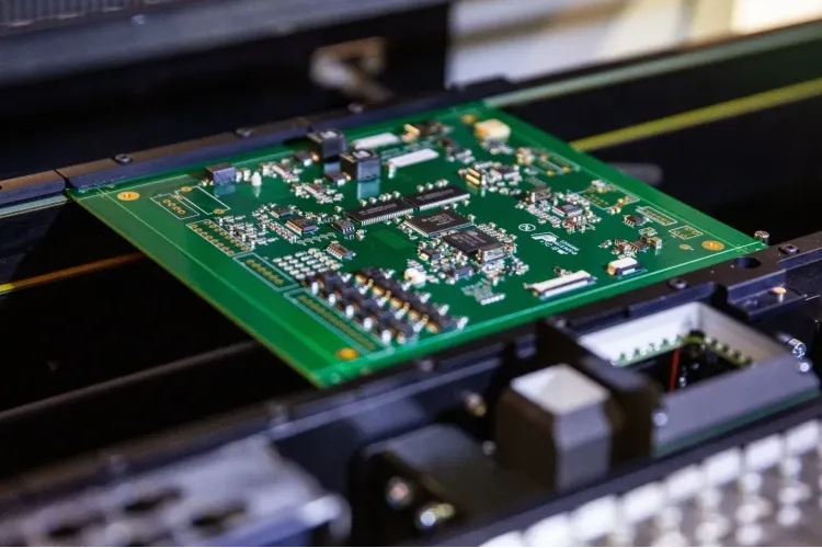
Printed Circuit Boards (PCBs) are the backbone of modern electronics, providing the physical platform for components to connect and function. A critical aspect of PCB design is creating accurate footprints—those copper pads and outlines that ensure components are correctly placed and soldered. However, even experienced engineers can make footprint errors that lead to manufacturing delays, costly rework, or outright board failure. In this blog, we explore the most common PCB footprint errors, their consequences, and practical steps to avoid them, empowering engineers to design reliable and efficient PCBs.
Whether you're working on a high-speed RF circuit or a compact IoT device, understanding these pitfalls can save time and resources. Let's dive into the key mistakes and how to steer clear of them.
What Are PCB Footprints and Why Do They Matter?
A PCB footprint, often called a land pattern, defines the physical interface between a component and the PCB. It includes copper pads for soldering, silkscreen markings for component identification, and other features like mounting holes or solder mask definitions. Each component, whether a surface-mount resistor, through-hole capacitor, or complex Ball Grid Array (BGA), requires a unique footprint tailored to its dimensions and pin configuration.
Footprint errors can disrupt the PCB assembly process, cause electrical failures, or render a board unusable. For example, a misaligned pad can prevent proper soldering, while an incorrect pin spacing might make a component incompatible with the board. According to industry data, design errors, including footprint mistakes, account for up to 60% of PCB prototype failures, highlighting their critical impact on project timelines and costs.
Common PCB Footprint Errors
Let's examine the most frequent footprint mistakes engineers encounter and their implications.
1. Incorrect Pad Size or Spacing
One of the most common errors is designing pads that are too small, too large, or incorrectly spaced for the component's pins. For instance, if a 0805 resistor's pads are spaced 0.5 mm apart instead of the required 0.8 mm, soldering becomes impossible, leading to poor connections or component misalignment. This issue often arises when engineers manually create footprints or use outdated component libraries.
Consequences
- Poor solder joints, increasing the risk of open circuits.
- Component misalignment, causing assembly delays.
- Potential tombstoning in surface-mount components, where one end lifts off the pad during reflow soldering.
How to Avoid
- Always verify pad dimensions against the component's datasheet. For example, IPC-7351B standards recommend a 1:1 ratio between copper pads and solder paste masks for most components.
- Use trusted CAD library parts from reputable sources like Ultra Librarian or SnapEDA, which align with industry standards.
- Perform a Design Rule Check (DRC) in your PCB design software to catch spacing errors early.
2. Misaligned Pin Numbering
Incorrect pin numbering, such as swapping pin 1 with another pin, can lead to catastrophic failures, especially for integrated circuits (ICs) like microcontrollers or transceivers. This error often occurs when the schematic symbol and footprint pin assignments don't match, causing the component to be oriented incorrectly during assembly.
Consequences
- Electrical shorts or open circuits, potentially damaging the component or board.
- Functional failure, as signals are routed to the wrong pins.
- Costly rework or scrapping of prototype boards.
How to Avoid
- Cross-check the footprint's pin assignments with the component's datasheet and schematic symbol.
- Use a clear pin 1 indicator (e.g., a dot or triangle) on the silkscreen layer to guide assembly.
- Leverage 3D PCB design tools to visualize component placement and orientation before fabrication.
3. Inadequate Clearance Between Pads
Placing pads too close together can cause the solder mask bridge, where solder unintentionally connects adjacent pins during reflow. This is particularly problematic for fine-pitch components like Quad Flat No-leads (QFNs) with pin pitches as small as 0.4 mm. Insufficient clearance also increases the risk of electrical shorts and signal interference.
Consequences
- Solder bridges leading to short circuits.
- Reduced signal integrity, especially in high-frequency circuits operating above 1 GHz.
- Increased manufacturing defects, lowering yield rates.
How to Avoid
- Follow IPC-7351B guidelines for minimum clearance, such as 6 mil (0.15 mm) for components smaller than 0603 packages and 39 mil (1 mm) for sensitive devices like BGAs.
- Incorporate solder mask dams (at least 1.6 mil wide) between pads to prevent solder flow.
- Run a Design for Manufacturability (DFM) check to identify clearance violations before sending files to the fabricator.
4. Incorrect Solder Paste Mask Design
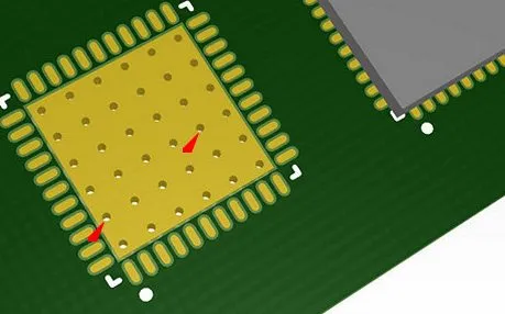
The solder paste mask defines where solder is applied during assembly. Errors like oversized or undersized paste masks can lead to uneven solder distribution, affecting joint reliability. For example, a QFN with a large exposed pad requires a segmented paste mask to prevent floating during reflow, but an incorrect design can cause voids or weak connections.
Consequences
- Solder voids, reducing thermal and electrical conductivity.
- Floating components, leading to misalignment or tombstoning.
- Increased risk of mechanical failure under thermal stress.
How to Avoid
- Segment large exposed pads (e.g., above 4 x 4 mm) into a symmetric array, as per IPC-7351B recommendations, to ensure even solder distribution.
- Verify solder paste mask dimensions against the component's datasheet and manufacturer's guidelines.
- Use PCB design software to preview solder paste application in 3D, ensuring alignment with pads.
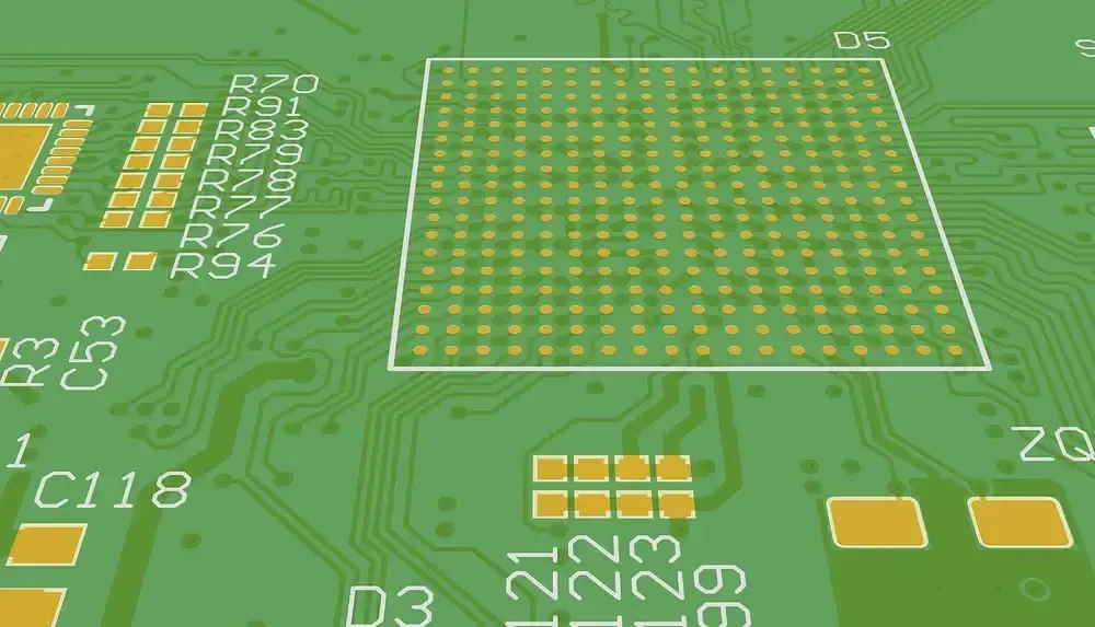
5. Ignoring Thermal Considerations
Footprints for high-power components, like power MOSFETs or LEDs, require adequate thermal reliefs to dissipate heat during soldering. Without proper thermal reliefs, heat can be drawn away too quickly, resulting in cold solder joints. Conversely, oversized thermal pads can cause excessive heat retention, damaging sensitive components.
Consequences
- Cold solder joints, leading to unreliable connections.
- Overheating, reducing component lifespan or causing failure.
- Warping of the PCB during reflow due to uneven thermal expansion.
How to Avoid
- Design thermal reliefs with spokes connecting pads to copper planes, typically 10-15 mil wide, to balance heat transfer.
- Place thermal vias under large pads to enhance heat dissipation, ensuring a minimum of 8 mil diameter for manufacturability.
- Simulate thermal performance using tools like Altium Designer's PDN Analyzer to optimize footprint design.
Best Practices for Flawless PCB Footprints
Beyond avoiding specific errors, adopting best practices can streamline the footprint creation process and enhance design reliability. Here are actionable tips to elevate your PCB design workflow:
1. Leverage Industry Standards
Adhering to standards like IPC-7351B ensures footprints are compatible with modern manufacturing processes. These guidelines cover pad sizes, clearances, and solder mask designs, reducing the risk of errors. For example, IPC recommends a minimum courtyard clearance of 10 mil (0.25 mm) around components to prevent interference during assembly.
2. Use Verified Component Libraries
Creating footprints from scratch is time-consuming and error-prone. Instead, use pre-verified libraries from platforms like DigiKey, Mouser, or PCB design software like KiCad and Altium Designer. These libraries are regularly updated to reflect component changes, ensuring accuracy.
3. Perform Rigorous Design Checks
Run DRC and DFM checks using your PCB design software to catch footprint errors before fabrication. These tools can identify issues like insufficient clearances, mismatched pin assignments, or improper solder mask definitions. Additionally, consider a peer review by another engineer to spot oversights.
4. Prototype and Test
Before full-scale production, fabricate a prototype to validate footprint accuracy. Test the board under real-world conditions, checking for soldering issues, thermal performance, and electrical connectivity. Tools like multimeters and oscilloscopes can help verify functionality.
5. Collaborate with Manufacturers Early
Engage with your PCB manufacturer during the design phase to ensure footprints align with their capabilities. For instance, some fabricators may require specific pad tolerances or solder mask thicknesses. Early collaboration can prevent costly revisions.
How ALLPCB Supports Flawless PCB Designs
At ALLPCB, we understand the challenges engineers face in creating error-free PCB footprints. Our advanced manufacturing capabilities and quick-turn prototyping services empower designers to iterate and refine their designs with confidence. With global logistics and a dedicated CAM engineering team, we provide comprehensive DFM checks to catch footprint errors before production, ensuring high yields and reliable boards. Whether you're designing a compact wearable or a complex industrial controller, ALLPCB's expertise helps you bring your vision to life efficiently and cost-effectively.
Conclusion
PCB footprint errors can derail even the most carefully planned projects, leading to delays, increased costs, and unreliable boards. By understanding common mistakes—like incorrect pad sizes, misaligned pins, and inadequate thermal reliefs—engineers can take proactive steps to ensure flawless designs. Leveraging industry standards, verified libraries, and rigorous design checks, combined with early collaboration with manufacturers, is key to success.
At ALLPCB, we're committed to supporting engineers with the tools and expertise needed to avoid these pitfalls. Start your next PCB project with confidence, knowing you have the knowledge and resources to create robust, high-quality designs.