 ALLPCB


In the modern industrial system, printed circuit boards (PCBs) are the cornerstone of electronic products. From simple household appliances to complex aerospace equipment, PCBs are everywhere, assuming the functions of connection, support and integrated circuits. With the advent of Industry 4.0, mass production of PCBs not only needs to meet the demand in terms of quantity, but also needs to integrate the new trends of intelligence, automation and informationization.
The process of industrial PCB production
Industrial PCB production is a complex and delicate process, which usually includes the following main steps:PCB Design
The first step in the PCB manufacturing process is PCB design. PCB design is created by professional designers using PCB design software such as Altium. This PCB design serves as a blueprint for the actual finished product.
PCB design is usually done by the customer, and then the design files are sent to the PCB manufacturer for production. The most widely used PCB design file format is the Gerber format. The Gerber file format is an open vector image file format that is the de facto industry standard.
Inspection and DFM Review
Once the manufacturer receives the PCB design files, the engineers conduct a second process inspection. The inspection process includes a DFM (Design for Manufacturability) review. During this process, trace widths, trace spacing, hole sizes, and other design parameters are verified. This is done to ensure that the design is error-free and meets the company's manufacturing capabilities.
Once the design is verified, multiple instances of the same design are grouped together to be manufactured on a single large panel. In this way, cost and complexity are reduced, and faster production is achieved.
Cleaning and Cutting
After the design verification and checking is completed, the large PCB boards are thoroughly dry cleaned to remove contaminants that may interfere with the manufacturing process or the quality of the PCB. The board pieces are then cut into smaller PCB panels suitable for manufacturing. The cutting and cleaning of the PCB boards is done using specialized machines.
Drilling
Once the larger PCB boards are cut into smaller panels, the next process step is to drill holes in these boards. Drilling serves two purposes. The first purpose of PCB drilling is to place through-hole components on the board. The second purpose of drilling is to create connections between the various copper layers of the PCB.
During the drilling process, the operator takes a piece of MDF (Medium Density Fiber) board and fixes the PCB panel on the MDF board. An aluminum sheet is also attached to the board as an entry foil, which enables burr-free drilling.
Once the sheet is prepared, it is fed into a computer-controlled machine that automatically drills holes in the PCB sheet as per the program. After the drilling process is completed, the sharp edges of the board are smoothed with a grinder.
Electroplating
The different copper layers on the PCB board are separated from each other by layers of non-conductive materials such as fiberglass. Therefore, in order to create connections between the isolated copper layers, the electroplating process is carried out.
During the electroplating process, the panel is immersed in an electrolyte. The copper on the panel acts as a cathode. A number of chemicals are used in this process. The entire process is controlled by a computer and a thin layer of copper is deposited in the drilled holes.
Printing
In this process step, a film with a printed circuit diagram is aligned on top of the PCB panel. The panel is then fed into a printer along with a UV lamp. The printer prints the circuit design on the film onto the PCB panel.
After printing the design onto the panel, the panel is treated with a chemical developer to remove unhardened residues.
Etching
The next process step in PCB manufacturing is etching. The purpose of this process is to remove unwanted copper from the board using an alkaline agent. After the copper is removed, the panel is washed to remove all chemicals.
Automated Optical Inspection
After etching, the panel is inspected and scrutinized using an automated optical inspection machine. The purpose of this inspection is to ensure quality standards to detect any errors that may have occurred during the previous process. The machine uses computer vision technology to scan the PCB panel and detect faults.
Solder Mask
The next process step is called solder masking. During this process, both sides of the PCB panel are coated with an epoxy solder mask. The solder mask protects the copper surface and prevents solder shorts between components. After the solder mask is applied, the PCB panel is dried and baked to secure the solder mask firmly.
Surface Finish
To protect the copper of the pads from oxidation, hot air solder leveling method is used for surface finish. Other surface finish methods include HASL, immersion gold, hard gold, and OSP.
Electrical Test
This is one of the last process steps during which all connections on the board are electrically tested as per the original board design. This automated testing method ensures that all connections are as per the original design and that there are no open or short circuits on the PCB.
Milling
This is the final process step which involves separating all the individual PCBs from the large panel. This process step is performed by a CNC milling machine. After cutting, the boards are again washed, cleaned and dried. Now the PCBs are vacuum sealed and bubble wrapped to protect against dust and moisture. These PCBs can now be shipped to the customer after proper packaging.
Key technologies in industrial PCB production
1. Multilayer board technology
With the increasing complexity of electronic product functions, the requirements for PCB wiring density and number of layers are getting higher and higher. Multilayer board technology effectively improves the integration and performance of PCB by superimposing multiple conductive layers on the substrate and realizing interlayer connection through vias.
2. High-density interconnect (HDI) technology
HDI technology uses processes such as micro blind holes and buried holes to further reduce the line width and spacing of PCBs, improve wiring density and signal transmission speed, and is suitable for the needs of high-end electronic products.
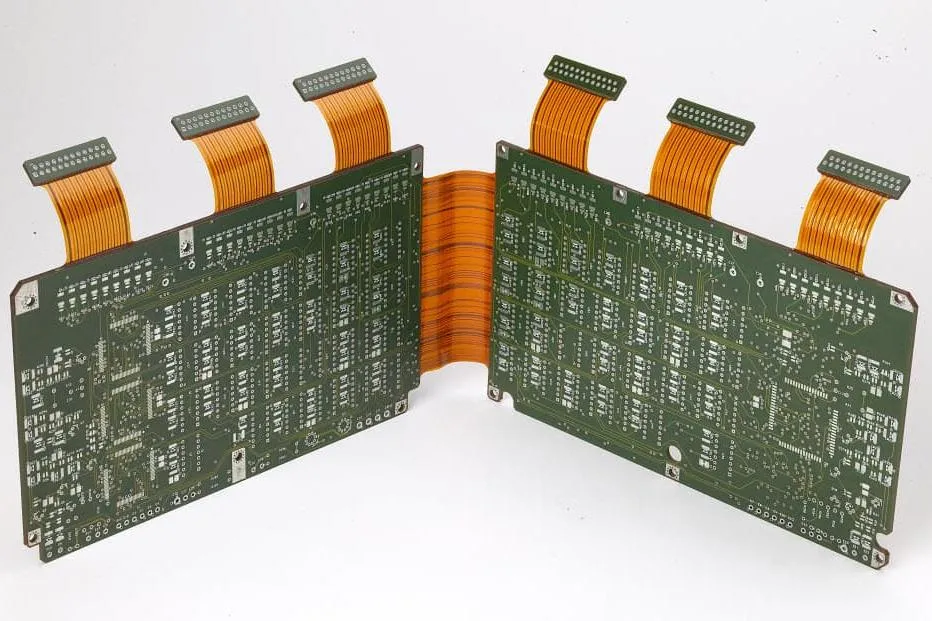
3. Rigid-flex technology
Rigid-flex combines rigid PCB and flexible PCB, which not only has the stability and support of rigid board, but also has the bendability and adaptability of flexible board, and is widely used in portable electronic devices and automotive electronics.
4. Lead-free process
For environmental protection and health considerations, lead-free process in PCB production has gradually become the mainstream. Lead-free welding requires higher welding temperature and stricter process control to ensure welding quality and reliability.
Development trend of industrial PCB production
1. Smaller, thinner and lighter
With the trend of miniaturization and portability of electronic products, PCB is also developing in the direction of smaller, thinner and lighter, which puts higher requirements on the precision of production process and the performance of materials.
2. Higher integration and performance
With the rapid development of technologies such as 5G communication, artificial intelligence, and the Internet of Things, the performance requirements for PCB signal transmission speed, frequency response, and anti-interference ability are constantly increasing, which has promoted the continuous innovation and upgrading of PCB technology.
3. Green and environmental protection
The increasingly stringent environmental regulations have prompted PCB manufacturers to adopt more environmentally friendly materials and processes, reduce the emission of harmful substances, and achieve sustainable development.
4. Intelligent manufacturing
The advent of the Industrial 4.0 era has made PCB production gradually move towards intelligent manufacturing. By introducing automated equipment, big data analysis and artificial intelligence technology, the production process can be optimized, quality can be monitored in real time, and predictive maintenance can be achieved.
Summary
As an important part of the electronics manufacturing industry, the continuous advancement and innovation of industrial PCB production technology plays a vital role in promoting the development of the electronic information industry. With the continuous development of science and technology and the continuous changes in market demand, PCB manufacturers need to continuously improve their technical level and innovation capabilities to adapt to the development trend of the industry and make greater contributions to the prosperity of the global electronic information industry.


